


Clamp Diodes: Principles, Protection Strategy, and Engineering Applications (2026)
Clamp diodes—also known as clampers or DC restorers—are circuits used to shift the DC level of a waveform without altering its shape. From an engineering standpoint, they serve two essential purposes:
- DC Restoration in AC-coupled signal chains
- Voltage limiting and transient protection for sensitive semiconductor nodes
In modern 3.3V and lower CMOS systems, clamp structures are fundamental to protecting microcontroller GPIO pins, ADC inputs, communication interfaces, and power switching devices from ESD events and voltage spikes.
Table of Contents
- 1. Engineering Fundamentals of Clamp Circuits
- 2. Protection-Oriented Clamping Architecture
- 3. GPIO Protection in Microcontrollers
- 4. Diode Selection Strategy (2026 Design Perspective)
- 5. Industrial Applications
- 6. FAQ
1. Engineering Fundamentals of Clamp Circuits
1.1 Core Operating Mechanism
A classical clamp circuit consists of:
- A diode (nonlinear conduction element)
- A capacitor (charge storage component)
- A resistor (discharge path defining time constant)
Operating Principle
During one half-cycle of the input signal:
- The diode becomes forward-biased.
- The capacitor charges to the peak value.
- The output node is fixed (clamped) to a reference potential.
During the opposite half-cycle:
- The diode becomes reverse-biased.
- The capacitor retains its stored charge.
- The stored voltage shifts the waveform vertically.
Design Requirement
To ensure minimal voltage droop:
RC >> T_signal
Where:
- RC = discharge time constant
- T_signal = signal period
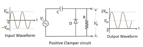
1.2 Negative Clamp Circuit
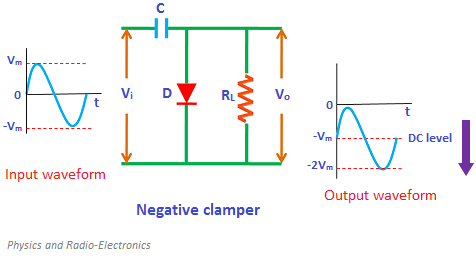
A negative clamp fixes the positive peak of the waveform to ground (or reference), shifting the entire signal downward.
Operation
Positive Half Cycle:
- Diode conducts.
- Capacitor charges to peak voltage Vp.
- Output ≈ 0V (ideal case).
Negative Half Cycle:
- Diode turns off.
- Capacitor maintains charge.
- Output becomes:
Vo = Vi − Vp
The peak-to-peak voltage remains unchanged. Only the DC reference shifts.
1.3 Biased Clamp Circuit
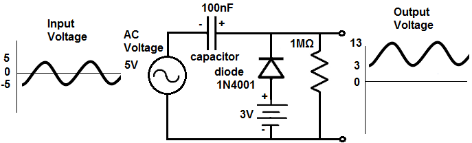
A biased clamp introduces a DC source Vref to define a non-zero clamp level.
Instead of clamping to 0V:
Vo = Vref
Applications include:
- ADC front-end biasing
- Video DC restoration
- Signal level shifting in mixed-signal systems
2. Protection-Oriented Clamping Architecture
Beyond waveform translation, clamp diodes are extensively used for transient containment.
A standard protection structure includes:
- Upper clamp diode connected to VDD
- Lower clamp diode connected to GND
- Series resistor for current limiting
Overvoltage Condition
If:
Vin > VDD + Vf
The upper diode conducts and diverts excess current into the supply rail.
Undervoltage Condition
If:
Vin < GND − Vf
The lower diode conducts and clamps the voltage toward ground.
This architecture confines the input node within safe operating limits.
3. GPIO Protection in Microcontrollers
Most modern microcontrollers integrate internal clamp diodes on every GPIO pin.
Internal Configuration
- Upper diode connected to VDD
- Lower diode connected to VSS
Electrical Envelope
VSS − 0.3V ≤ Vin ≤ VDD + 0.3V
Internal clamp diodes are primarily intended for ESD events, not continuous current conduction.
If external signals may exceed supply rails:
- Add a series resistor (typically 1kΩ to 10kΩ)
- Use external Schottky clamp diodes
4. Diode Selection Strategy (2026 Design Perspective)
When designing clamp protection networks, engineers should consider:
- Forward voltage (Vf): Must be lower than the internal diode drop.
- Reverse recovery time: Critical for fast transients.
- Junction capacitance: Impacts high-speed signal integrity.
- Surge current rating: Must withstand IEC ESD pulses.
Schottky diodes are preferred because they offer fast switching, low forward voltage, and reduced stress on internal silicon structures.
5. Industrial Applications
Clamp diodes are widely used in:
High-Speed Digital Systems:
- Protecting MCU and FPGA inputs
- USB, CMOS, and LVDS interfaces
Switching Power Supplies:
- Limiting MOSFET drain-source voltage spikes
- Suppressing transformer leakage inductance effects
Video and Display Systems:
- DC restoration to prevent image drift
- AC-coupled signal stabilization
Measurement and Instrumentation:
- Oscilloscope front-end protection
- Precision amplifier input safeguarding
6. FAQ
What is the difference between a Clipper and a Clamper?
A clipper removes part of a waveform and alters its shape by limiting amplitude.
A clamper shifts the entire waveform up or down without changing its shape.
Does clamping change peak-to-peak voltage?
No. A properly designed clamping circuit only shifts the DC offset.
Example:
Input: 10Vpp sine wave (−5V to +5V)
Clamped at 0V → Output becomes 0V to +10V
The amplitude remains 10Vpp.
Why are Schottky diodes preferred in modern protection designs?
They conduct earlier due to lower forward voltage, switch faster, reduce stress on internal ESD structures, and improve survivability during IEC ESD testing.
Engineering Conclusion
Clamp diodes are foundational elements in modern electronic systems. Whether performing DC restoration in signal processing chains or protecting low-voltage CMOS inputs from destructive voltage excursions, their correct implementation directly impacts system robustness and reliability.
In advanced circuit design, clamping must be treated not as an afterthought but as a deliberate part of the overall signal integrity and protection architecture.