


Common PCB Solder Bridge Problems and Engineering Mitigation Strategies
Solder bridging is a high-frequency defect mechanism in PCB assembly, particularly in fine-pitch surface mount technology (SMT). It introduces unintended conductive paths that degrade signal integrity, cause functional failures, and reduce long-term reliability. This article analyzes solder bridge formation from a process engineering perspective, covering wetting dynamics, design constraints, process control variables, inspection methodologies, and rework techniques. It emphasizes practical, production-grade mitigation strategies aligned with IPC standards and modern high-density PCB manufacturing.
Table of Contents
- 1. What Is a Solder Bridge
- 2. Formation Mechanism and Physics
- 3. High-Risk Scenarios in Modern PCB Design
- 4. Solder Mask Engineering Constraints
- 5. Root Cause Analysis (RCA)
- 6. Process Control in SMT and THT
- 7. Design for Manufacturability (DFM) Guidelines
- 8. Inspection and Defect Detection Technologies
- 9. Controlled Rework and Defect Removal
- 10. Conclusion
- FAQ
1. What Is a Solder Bridge
A solder bridge is an unintended metallurgical connection between two adjacent conductive features—pads, leads, or traces—on a PCB. Unlike designed solder jumpers, these defects violate electrical isolation constraints defined in the netlist.
From an electrical standpoint, solder bridges introduce:
- Hard shorts (low impedance paths)
- Leakage currents
- Crosstalk in high-speed circuits
- Intermittent faults under thermal cycling
2. Formation Mechanism and Physics
2.1 Wetting Behavior and Surface Energy
Molten solder follows wetting principles governed by surface energy minimization. It preferentially spreads over clean copper pads and metallized component leads. However, excessive solder volume or reduced inter-pad spacing allows solder to extend beyond intended boundaries.
2.2 Capillary Action in Fine Pitch Geometry
In fine-pitch devices (<0.5 mm pitch), capillary forces between leads can actively pull molten solder into narrow gaps, significantly increasing bridge probability.
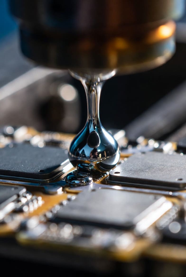
Figure 1: Molten solder spreading across adjacent pads due to excessive volume and capillary forces.
3. High-Risk Scenarios in Modern PCB Design
3.1 Fine Pitch Components
Devices such as QFP, QFN, BGA, TSOP, and high-pin-count microcontrollers present minimal spacing, making process tolerance extremely tight.
3.2 High-Density Interconnect (HDI)
HDI boards introduce microvias, ultra-fine traces, and dense pad arrays, reducing solder confinement margins and increasing bridging risks.
3.3 Reflow Profile Sensitivity
Improper thermal profiling can increase solder fluidity or result in incomplete wetting, both contributing to defect formation.
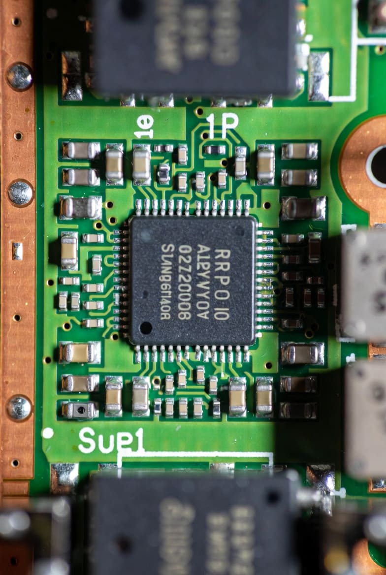
Figure 2: Solder bridging risk in fine-pitch IC leads with insufficient spacing.
4. Solder Mask Engineering Constraints
4.1 Solder Mask Dam Design
The solder mask acts as both a physical barrier and a surface energy modifier to confine molten solder.
Key parameters:
- Minimum dam width: 75–100 µm (3–4 mil)
- Alignment tolerance: ±25 µm
Failure modes include mask misregistration, insufficient dam width, and degradation during thermal cycling.
4.2 Pad Definition Strategy
| Pad Type | Description | Advantages | Risks |
|---|---|---|---|
| NSMD (Non-Solder Mask Defined) | Pad defined by copper, mask opening larger than pad | Better solder joint reliability | Higher solder bridging risk |
| SMD (Solder Mask Defined) | Pad defined by solder mask opening | Improved solder confinement | Lower mechanical strength |
5. Root Cause Analysis (RCA)
5.1 Material Factors
- Excess solder paste deposition
- Low-viscosity flux promoting spread
- Oxidized pads affecting wetting
5.2 Process Factors
- Excessive stencil thickness
- Poor aperture design
- Placement misalignment
- Improper thermal profile
5.3 Human Factors
- Excess solder feeding
- Improper soldering angle
- Lack of temperature control
6. Process Control in SMT and THT
| Process | Control Parameter | Impact on Solder Bridging |
|---|---|---|
| Solder Paste Printing | Stencil thickness, aperture size | Directly controls solder volume |
| Component Placement | Alignment accuracy | Prevents lead overlap |
| Reflow Soldering | Thermal profile | Controls solder fluidity |
| Wave Soldering | Wave height, conveyor angle | Affects solder flow direction |
Typical soldering temperatures:
- Leaded solder: 330°C – 350°C
- Lead-free solder: 350°C – 380°C
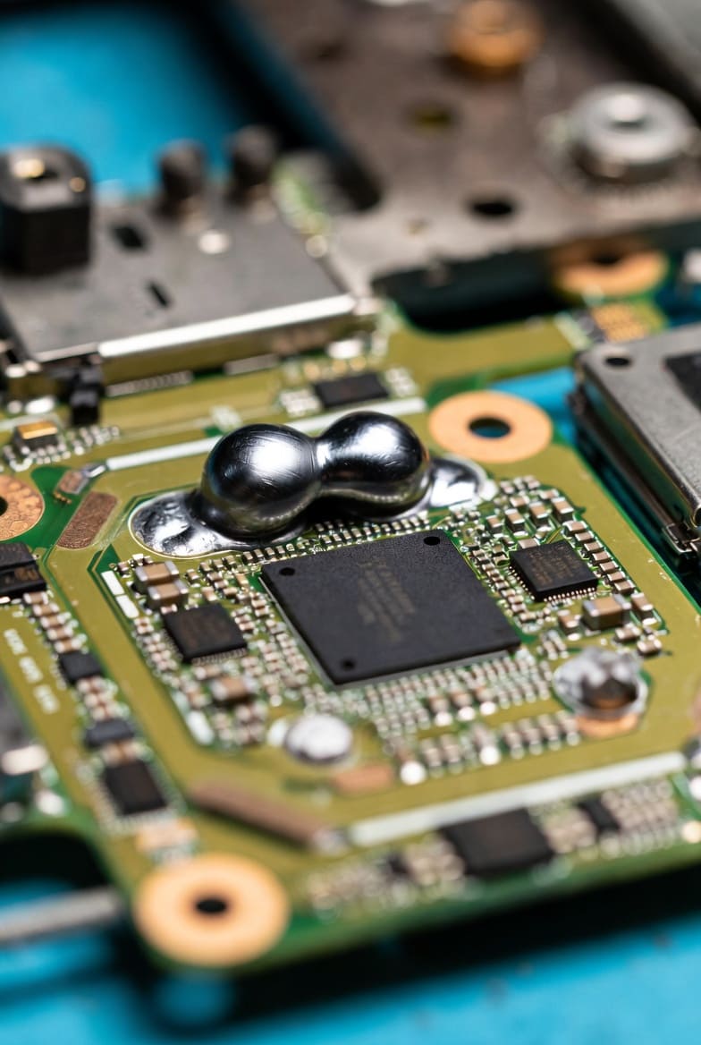
Figure 3: Improper reflow profile causing excessive solder flow and bridging.
7. Design for Manufacturability (DFM) Guidelines
7.1 Pad Geometry Optimization
- Avoid oversized pads
- Maintain uniform spacing
- Implement solder thieving when necessary
7.2 Stencil Design Optimization
- Apply aperture reduction (10–20%)
- Use home plate design for fine pitch
- Apply step-down stencil for dense regions
7.3 Placement Accuracy
- Use high-precision pick-and-place machines (±25 µm)
- Apply fiducial alignment systems
8. Inspection and Defect Detection Technologies
| Inspection Method | Capability | Limitation |
|---|---|---|
| Visual Inspection | Quick detection of visible defects | Operator-dependent |
| AOI | Automated high-speed detection | Cannot detect hidden joints |
| X-ray Inspection | Detects hidden bridges (BGA/QFN) | Higher cost |
| Electrical Testing | Functional verification | Does not localize defect visually |
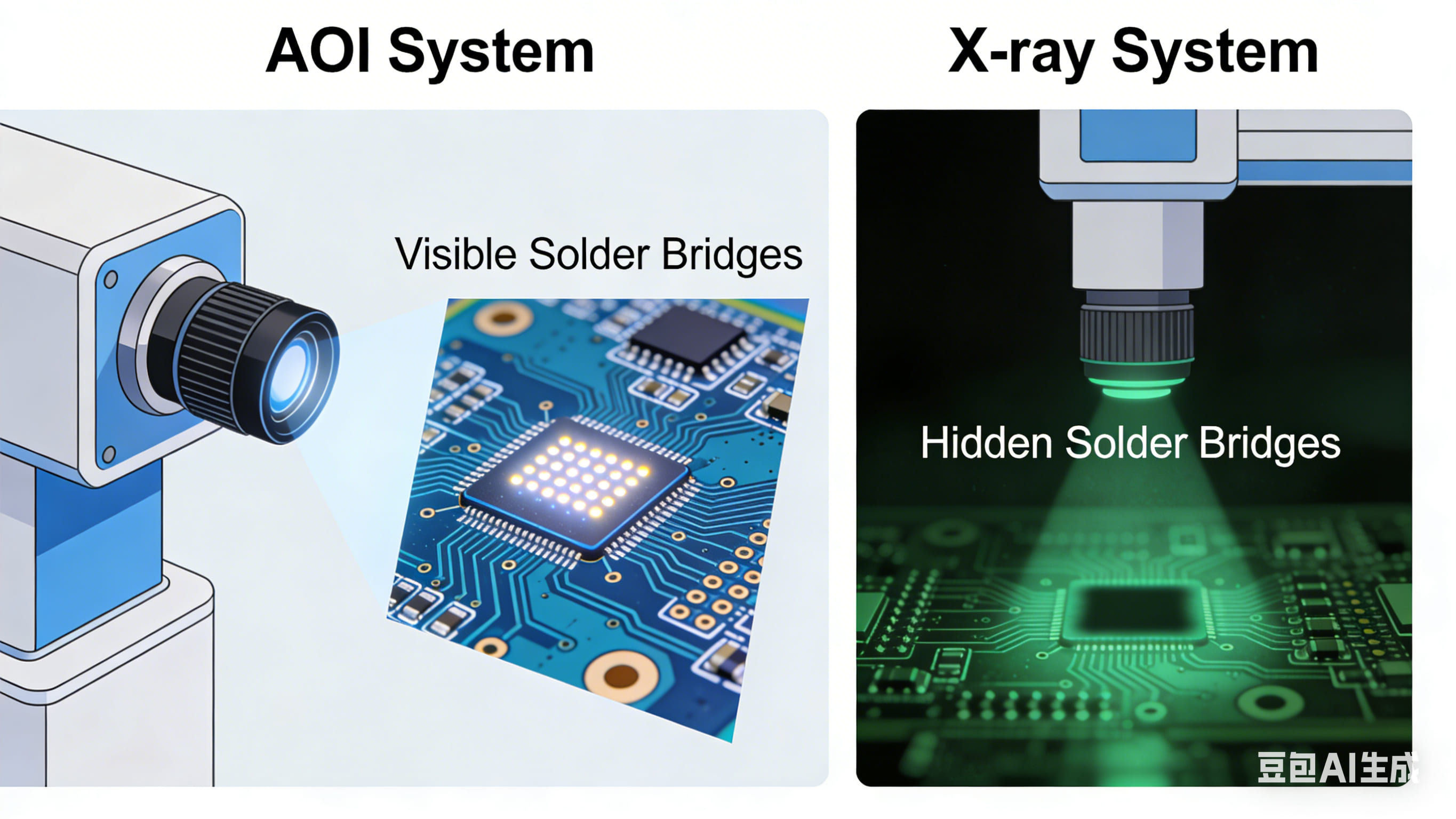
Figure 4: AOI and X-ray systems detecting visible and hidden solder bridges.
9. Controlled Rework and Defect Removal
9.1 Solder Wick (Desoldering Braid)
Absorbs molten solder through capillary action; requires flux for efficiency.
9.2 Hot Air Rework
Provides localized heating for solder reflow and component repositioning.
9.3 Desoldering Pump
Suitable for removing large solder volumes, especially in through-hole assemblies.
9.4 Rework Risks
- Pad delamination
- Thermal damage to components
- Repeated defect formation if root cause is not eliminated
10. Conclusion
Solder bridges are predictable and preventable defects arising from insufficient control over materials, geometry, and process parameters. In high-density PCB manufacturing, effective mitigation requires integration of DFM practices, controlled soldering processes, and advanced inspection technologies. A systematic engineering approach ensures improved yield, reliability, and long-term performance of electronic assemblies.
FAQ
Q1: Why are solder bridges more common in lead-free processes?
Lead-free alloys have higher surface tension and melting temperatures, making them more sensitive to process variations and increasing bridging risk.
Q2: What is the most effective prevention strategy?
A combined approach including stencil optimization, solder paste control, accurate placement, and proper reflow profiling is required.
Q3: Can AOI detect all solder bridges?
No. AOI detects visible defects only. Hidden bridges require X-ray inspection.
Q4: Is manual soldering reliable for fine-pitch components?
Only with skilled operators, precision tools, and magnification. Otherwise, defect rates increase significantly.
Q5: What standard defines solder bridge defects?
IPC-A-610 defines solder bridges as defects across all product classes and requires corrective action.