


CPU Manufacturing Process for Modern Processors: From Silicon to Advanced Microarchitecture
The Central Processing Unit (CPU) is the core computing component of modern electronic systems. From personal computers and smartphones to servers and industrial controllers, CPUs execute instructions, process data, and coordinate system operations. Modern processors integrate tens of billions of transistors fabricated at nanometer scale using advanced semiconductor manufacturing technologies.
CPU fabrication is one of the most complex industrial processes in the world. It involves ultra-pure materials, atomic-level doping, extreme ultraviolet lithography (EUV), multilayer interconnect structures, and high-precision testing and packaging technologies.
This article explains the complete CPU manufacturing process, starting from silicon purification and wafer preparation to transistor formation, circuit patterning, metal interconnection, testing, binning, and packaging. The goal is to provide a clear technical overview of how modern processors are designed and manufactured.
Table of Contents
- 1. What Is a CPU (Central Processing Unit)?
- 2. Core Materials Used in CPU Fabrication
- 3. Silicon Purification and Single-Crystal Ingot Growth
- 4. Photolithography and EUV Patterning Technology
- 5. Ion Implantation and Semiconductor Doping
- 6. Metal Interconnects and Multilayer Circuit Integration
- 7. Wafer Testing, Dicing, and Processor Binning
- 8. Step-by-Step CPU Manufacturing Flow
- 9. Major Applications of CPUs
- 10. FAQ
- 11. Conclusion
1. What Is a CPU (Central Processing Unit)?
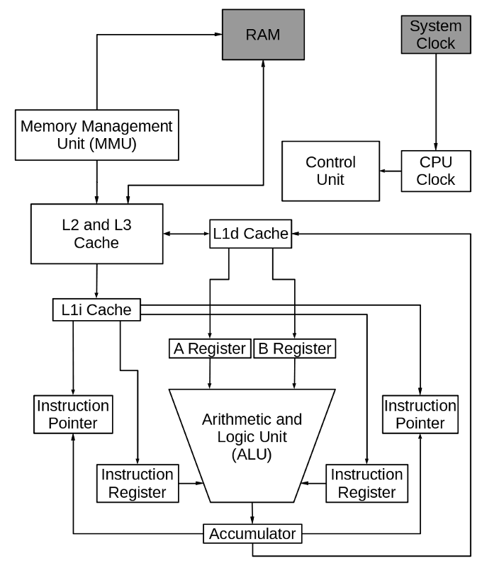
A Central Processing Unit (CPU) is the primary computational engine inside digital systems. It reads program instructions, processes data, and controls communication between different hardware components.
Modern CPUs consist of multiple functional units including:
- Processing cores responsible for executing instructions
- Instruction pipelines that improve execution throughput
- Cache memory (L1, L2, L3) that reduces memory latency
- Branch prediction logic to optimize program flow
- Memory controllers that interface with system RAM
At the physical level, CPUs are built using CMOS transistors. These microscopic switches control electrical current to perform logical operations.
Modern processors may contain 10 to 100 billion transistors, each switching billions of times per second. These transistors are interconnected through extremely complex wiring layers that form the processor’s logic circuits.
2. Core Materials Used in CPU Fabrication
CPU manufacturing requires several specialized materials designed for semiconductor fabrication.
Silicon (Si)
Silicon is the fundamental material used to build semiconductor devices because its electrical conductivity can be precisely controlled.
Key advantages include:
- Stable semiconductor properties
- Ability to form high-quality insulating oxide (SiO₂)
- Compatibility with large-scale manufacturing processes
High-purity silicon used in chip fabrication reaches 99.9999999% purity (9N).
Silicon Dioxide (SiO₂)
Silicon dioxide serves as a dielectric insulating layer in semiconductor devices. It separates conductive elements and acts as a gate oxide in transistor structures.
Copper
Copper is widely used for interconnect wiring due to its low electrical resistance and superior signal transmission properties compared with aluminum.
Dopant Elements
Semiconductor conductivity is adjusted by introducing small amounts of impurities known as dopants.
| Dopant | Type | Function |
|---|---|---|
| Boron | P-type | Creates holes for positive charge carriers |
| Phosphorus | N-type | Adds extra electrons to the silicon lattice |
| Arsenic | N-type | Used for shallow high-precision doping |
These dopants enable the creation of P-type and N-type semiconductor regions, which are essential for transistor operation.
3. Silicon Purification and Single-Crystal Ingot Growth
The manufacturing process begins with silicon extracted from quartz sand (SiO₂).
Silicon Refinement
Quartz undergoes carbothermic reduction:
SiO₂ + 2C → Si + 2CO
This reaction converts silicon dioxide into elemental silicon using carbon as the reducing agent. The process produces metallurgical-grade silicon, which still contains impurities and must be further refined.
To achieve semiconductor-grade purity, the material is further refined using chemical processes such as the Siemens purification process, which produces ultra-high-purity polysilicon.
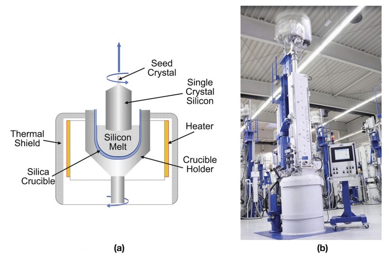
Single-Crystal Ingot Growth
Processors require monocrystalline silicon. The most common growth method is the Czochralski process.
Steps include:
- Silicon is melted at approximately 1420°C
- A seed crystal is inserted into the melt
- The crystal is slowly pulled upward while rotating
- A cylindrical single crystal forms
Modern semiconductor ingots can reach 300 mm in diameter, which allows manufacturers to produce many chips from a single wafer.
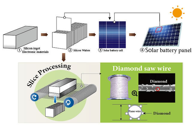
Wafer Production
The ingot is sliced into thin wafers using precision diamond saws. These wafers are then polished through chemical-mechanical processes to create a mirror-smooth surface required for nanometer-scale lithography.
4. Photolithography and EUV Patterning Technology
Photolithography is used to transfer microscopic circuit patterns onto silicon wafers.
Lithography Process
- A light-sensitive photoresist layer is applied to the wafer
- A photomask containing the circuit pattern is aligned
- Ultraviolet light exposes the pattern onto the wafer
- Chemical development reveals the pattern
- Etching removes selected material areas
This process is repeated dozens of times to construct the full circuit layout.
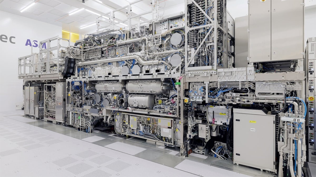
EUV Lithography
Advanced semiconductor nodes rely on Extreme Ultraviolet Lithography (EUV).
Key characteristics include:
- Wavelength: 13.5 nm
- Enables features smaller than 10 nm
- Uses reflective mirror optics rather than lenses
EUV enables fabrication of advanced transistor structures such as FinFET and Gate-All-Around (GAAFET) devices, which improve energy efficiency and transistor density.
5. Ion Implantation and Semiconductor Doping
After circuit patterns are defined, the electrical properties of silicon must be modified.
Ion Implantation
Ion implantation introduces dopant atoms into the silicon lattice by accelerating them using electric fields.
Typical parameters include:
- Implant energy: 10 keV – several MeV
- Dopant dose: 10¹¹ – 10¹⁵ ions/cm²
Formation of PN Junctions
By doping different regions with boron or phosphorus, engineers create P-type and N-type semiconductor regions.
These regions form PN junctions, which are fundamental components of semiconductor devices such as:
- diodes
- MOSFET transistors
After implantation, wafers undergo thermal annealing to repair crystal damage and activate dopants.
6. Metal Interconnects and Multilayer Circuit Integration
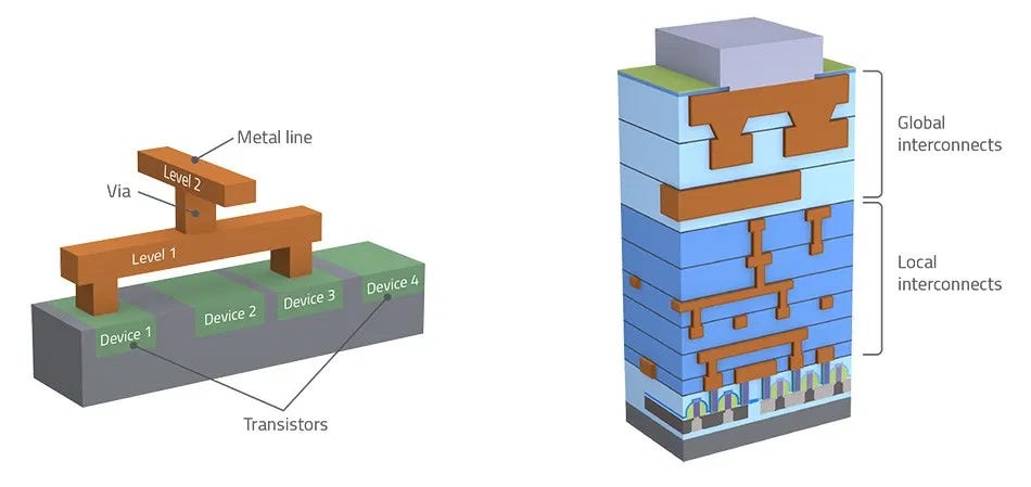
Once transistors are created, they must be connected to form functional circuits.
Modern processors use multilayer metal interconnect networks.
Interconnect Structure
Typical CPUs contain:
- 10–15 metal layers
- billions of vertical connections (vias)
These structures allow signals to travel across the chip between different logic blocks.
Dielectric Layers
Insulating materials called low-k dielectrics are placed between metal layers to reduce electrical interference and capacitance.
Chemical Mechanical Planarization (CMP)
CMP polishing ensures each layer remains flat so that subsequent lithography steps maintain nanometer-scale accuracy.
7. Wafer Testing, Dicing, and Processor Binning
After fabrication, the wafer undergoes extensive testing.
Wafer Probe Testing
Electrical probes test each chip while still on the wafer to detect defects and verify functionality.
Wafer Dicing
The wafer is cut into individual chips called dies using precision cutting equipment.
Chip Packaging
Each die is mounted onto a package substrate and connected using:
- flip-chip solder bumps
- wire bonding
A metal heat spreader is added to improve thermal dissipation.
Performance Binning
Due to manufacturing variations, processors are sorted into performance categories.
For example:
- high-frequency chips become premium models
- partially functional chips become lower-tier CPUs
This binning process improves manufacturing efficiency and product segmentation.
8. Step-by-Step CPU Manufacturing Flow
The simplified CPU manufacturing workflow includes:
- Quartz sand extraction
- Silicon purification
- Single-crystal ingot growth
- Wafer slicing
- Wafer polishing
- Photoresist coating
- Photolithography patterning
- Plasma etching
- Ion implantation
- Transistor formation
- Metal interconnect deposition
- Planarization (CMP)
- Wafer electrical testing
- Die separation
- Chip packaging
- Performance binning
In real semiconductor fabrication plants, the full process may involve over 1,000 individual manufacturing steps.
9. Major Applications of CPUs
CPUs are used across many types of electronic systems.
Personal Computers
Desktop and laptop processors run operating systems, applications, and software tools.
Data Centers
Server CPUs power cloud computing infrastructure, virtualization systems, and large-scale databases.
Mobile Devices
Smartphones integrate CPUs within System-on-Chip (SoC) architectures.
Embedded Systems
Processors control industrial equipment, networking devices, and smart appliances.
Automotive Electronics
Modern vehicles use processors to manage engine control, safety systems, and infotainment platforms.
10. FAQ
How many transistors are in a modern CPU?
Advanced processors fabricated using 5 nm or 3 nm process nodes can contain tens of billions of transistors.
Why is silicon used for processors?
Silicon offers stable semiconductor behavior, excellent thermal properties, and the ability to form high-quality oxide layers for transistor gates.
What is EUV lithography?
EUV lithography uses 13.5-nanometer wavelength light to create extremely small circuit features required for advanced semiconductor nodes.
Why are CPUs sold at different performance levels?
Manufacturing variations cause chips to perform differently. Through binning, manufacturers categorize processors based on maximum frequency and power efficiency.
11. Conclusion
The CPU manufacturing process represents one of the most advanced engineering achievements in modern technology. Starting from quartz sand, semiconductor fabrication techniques transform raw materials into highly sophisticated integrated circuits containing billions of nanoscale transistors.
Through innovations such as EUV lithography, atomic-level doping, multilayer copper interconnects, and advanced packaging technologies, manufacturers can produce processors capable of executing trillions of operations per second.
Although a CPU appears small in size, it embodies decades of semiconductor research and industrial innovation. Understanding how CPUs are manufactured helps reveal the remarkable engineering behind the digital devices that power modern society.