


LGA vs BGA: Engineering Guide to Chip Package Selection
Chip packaging plays a critical role in electrical performance, thermal management, mechanical reliability, and product serviceability. Among modern semiconductor packages, Land Grid Array (LGA) and Ball Grid Array (BGA) are two dominant technologies used across CPUs, embedded systems, mobile electronics, and automotive modules.
This article explains the engineering structure, assembly process, electrical characteristics, reliability considerations, and real-world applications of LGA and BGA packages. It also provides practical guidance for hardware designers on how to select the appropriate package based on signal integrity, thermal performance, mechanical constraints, and maintainability.
Table of Contents
- 1. Introduction to Modern IC Packaging
- 2. Land Grid Array (LGA)
- 3. Ball Grid Array (BGA)
- 4. Structural and Electrical Differences Between LGA and BGA
- 5. Mechanical Reliability and Thermal Behavior
- 6. Assembly, Soldering, and Inspection Methods
- 7. Typical Application Scenarios
- 8. Package Height and System Integration
- 9. Engineering Guidelines for Choosing LGA or BGA
- 10. FAQ
- 11. Conclusion
1. Introduction to Modern IC Packaging
Integrated circuit packaging provides three essential engineering functions:
- Electrical interconnection between silicon die and PCB
- Mechanical protection of the semiconductor die
- Thermal path for heat dissipation
As integrated circuits increase in complexity, traditional leaded packages such as QFP struggle to support the high pin counts, high speed signals, and compact layouts required by modern electronics.
To address these limitations, area array packaging technologies such as LGA and BGA distribute connections across the entire underside of the chip, significantly increasing connection density and improving electrical performance.
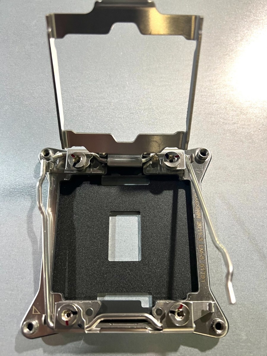
2. Land Grid Array (LGA)
2.1 LGA Structural Design
A Land Grid Array (LGA) package uses flat conductive pads (lands) arranged in a grid on the underside of the package substrate. These pads connect either to:
- Spring-loaded socket pins, or
- Direct solder joints to PCB pads.
In desktop and server systems, the pins are located in the socket rather than on the processor, reducing the risk of damaging the expensive CPU during handling.
A widely used variation is Flip-Chip LGA (FCLGA). In this architecture:
- The silicon die is flipped upside down.
- Micro solder bumps connect the die to the package substrate.
- Heat spreads more efficiently through the backside of the die.
This configuration reduces interconnect inductance and signal path length, improving high-speed performance.
Key Structural Elements
- Organic package substrate
- Copper redistribution layers
- Nickel-gold plated contact lands
- Optional integrated heat spreader (IHS)
2.2 Electrical and Thermal Characteristics
LGA packages offer several electrical advantages:
Low inductance contacts
Shorter signal paths reduce parasitic inductance, beneficial for high-frequency interfaces such as PCIe and memory buses.
High current capability
Large contact pads allow better power distribution networks (PDN), enabling modern CPUs to draw over 200 A transient current.
Thermal performance
Heat is transferred directly from die → heat spreader → heatsink, providing excellent cooling capability in server systems.
3. Ball Grid Array (BGA)
3.1 BGA Structural Design
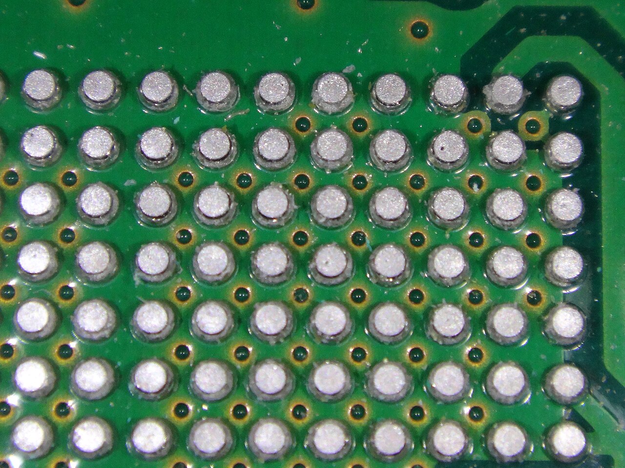
A Ball Grid Array (BGA) package uses an array of solder balls on the underside of the device as electrical connections.
During manufacturing:
- Solder paste is applied to PCB pads
- The BGA device is placed using pick-and-place equipment
- The board passes through a reflow oven
- Solder balls melt and form permanent joints
Because the connections are located underneath the package, BGA supports much higher I/O density than leaded packages.
Internal Package Structure
Typical BGA layers include:
- Silicon die
- Bond wires or flip-chip bumps
- Organic laminate substrate
- Solder mask
- Solder ball array
3.2 Electrical and Thermal Characteristics
BGA offers several performance advantages:
High connection density
Thousands of I/O connections can be integrated into a compact footprint.
Excellent signal integrity
Shorter vertical interconnects reduce impedance discontinuities and electromagnetic interference.
Improved thermal conduction
Heat can dissipate through both the package top and the solder ball array into the PCB.
These characteristics make BGA ideal for mobile processors, GPUs, and high-speed memory.
4. Structural and Electrical Differences Between LGA and BGA
| Feature | LGA | BGA |
|---|---|---|
| Contact Type | Flat pads | Solder balls |
| Attachment Method | Socket or solder | Reflow soldering |
| Replaceability | Replaceable when socketed | Permanent |
| Signal Density | High | Very high |
| Repair Difficulty | Moderate | High |
| Inspection | Visual + X-ray | Mostly X-ray |
The fundamental difference is that LGA separates the electrical contact from the solder joint, while BGA integrates them into a single solder ball structure.
5. Mechanical Reliability and Thermal Behavior
.jpg)
Mechanical reliability depends heavily on thermal cycling and mechanical stress.
BGA Reliability Considerations
BGA solder joints are exposed to thermal expansion mismatch between:
- silicon die
- package substrate
- PCB material
Repeated temperature cycles can cause solder fatigue cracking.
To mitigate this, designers often use:
- Underfill materials
- High Tg PCB laminates
- Optimized solder alloy compositions
LGA Reliability Considerations
LGA sockets avoid solder fatigue because the connection is mechanical rather than metallurgical. However, they introduce other risks:
- Bent socket pins
- Contact resistance variation
- Reduced reliability in high-vibration environments
Therefore LGA sockets are typically used in controlled environments such as servers and desktops.
6. Assembly, Soldering, and Inspection Methods
Manufacturing processes differ significantly between the two packages.
LGA Assembly
Two approaches exist:
Socketed LGA
- CPU inserted into socket
- Load plate secures contact pressure
- Allows field replacement
Direct-solder LGA
- Solder paste applied to PCB pads
- Package reflow soldered similar to QFN
BGA Assembly
BGA packages require precise SMT processes:
- stencil printing
- pick-and-place alignment
- reflow temperature profiling
Inspection typically involves:
- Automated Optical Inspection (AOI)
- X-ray inspection
Because solder joints are hidden under the package.
7. Typical Application Scenarios
LGA Applications
- Desktop processors
- Enterprise server CPUs
- High-end workstations
- Networking equipment
These systems benefit from serviceability and upgrade capability.
BGA Applications
- Smartphones
- Tablets
- GPUs
- DRAM and flash memory
- Automotive ECUs
- Embedded computing modules
These systems prioritize compact design and high integration.
8. Package Height and System Integration
| Category | LGA | BGA |
|---|---|---|
| Component Height | Moderate | Low |
| Socket Impact | Adds 3–6 mm | None |
| PCB Density | Medium | High |
| Device Profile | Taller | Very compact |
For ultra-thin devices, BGA is usually the only practical option.
9. Engineering Guidelines for Choosing LGA or BGA
Hardware designers typically evaluate four factors:
1. Serviceability
If the processor must be replaceable or upgradeable, choose LGA.
2. Board Space
For compact PCB layouts, BGA offers superior I/O density.
3. Thermal Management
High-power processors often use LGA with large heat spreaders.
4. Manufacturing Complexity
BGA requires more advanced SMT process control and inspection capability.
10. FAQ
Why do laptops usually use BGA processors?
Laptops prioritize thin form factors and compact PCB layouts, which BGA packages enable by eliminating sockets.
Are BGA chips impossible to replace?
No. They can be replaced using BGA rework stations, but the process requires specialized equipment and skilled technicians.
Why do desktop CPUs still use LGA?
Desktop systems value upgradeability and serviceability, allowing users to replace processors without soldering.
Which package provides better signal integrity?
Both can perform well. However, BGA often provides shorter signal paths, which is advantageous for very high-speed interfaces.
11. Conclusion
LGA and BGA represent two mature but fundamentally different packaging strategies.
- LGA prioritizes serviceability, power delivery, and high-performance cooling.
- BGA focuses on miniaturization, integration density, and manufacturing efficiency.
Understanding their structural differences, assembly requirements, and reliability characteristics allows engineers to select the most appropriate package for their system architecture, mechanical constraints, and lifecycle requirements.