


How Transistor Biasing Works and Why Stability Matters in BJT Amplifier Design
Transistor biasing is a fundamental concept in analog circuit design that determines whether an amplifier operates linearly or produces distortion. Proper biasing establishes a stable quiescent operating point (Q point), while stabilization techniques ensure that this operating point remains consistent despite variations in temperature, transistor gain (β), power supply fluctuations, and component tolerances.
This article provides a technical engineering perspective on BJT biasing. It explains Q-point control, common emitter bias structures, feedback mechanisms, and the physics behind thermal runaway. Practical biasing strategies used in real amplifier circuits are also analyzed to help engineers design stable and reliable transistor stages.
Table of Contents
- Understanding Transistor Biasing and Stability
- BJT Operating Regions and Q-Point Placement
- Basic Transistor Bias Circuit Architecture
- Biasing in a Common Emitter Amplifier
- Major Types of BJT Biasing Circuits
- Thermal Runaway Mechanism and Prevention
- Engineering Applications of Biasing Techniques
- Advantages and Limitations of Transistor Biasing
- FAQ
- Conclusion
1. Understanding Transistor Biasing and Stability
Transistor biasing is the process of establishing fixed DC voltages and currents in a transistor circuit before any signal is applied. These DC conditions define the quiescent operating point (Q-point).
The Q-point specifies three critical values:
- Base current (IB)
- Collector current (IC)
- Collector-Emitter voltage (VCE)
These values determine where the transistor sits on its DC load line.
For linear amplification, the transistor must operate in the active region. If the Q-point moves toward:
- Cutoff region → signal clipping at the lower side
- Saturation region → signal clipping at the upper side
the amplifier produces distortion.
Biasing vs Stabilization
| Aspect | Biasing | Stabilization |
|---|---|---|
| Definition | Establishes DC operating point | Maintains operating point stability |
| Primary Goal | Set Q-point | Prevent drift |
| Influencing Factors | Resistor network, supply voltage | Temperature, β variation |
| Impact | Enables amplification | Ensures consistent performance |
In practice:
Biasing defines the operating point, while stabilization keeps it from moving.
2. BJT Operating Regions and Q-Point Placement
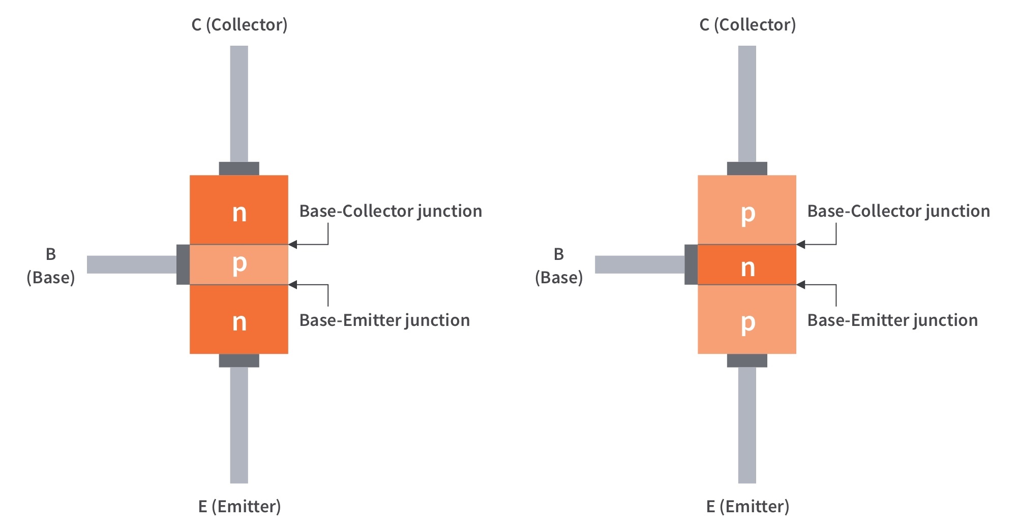
A Bipolar Junction Transistor (BJT) operates in three regions:
| Region | Base-Emitter Junction | Collector-Base Junction | Application |
|---|---|---|---|
| Cutoff | Reverse biased | Reverse biased | Switch OFF |
| Active | Forward biased | Reverse biased | Amplification |
| Saturation | Forward biased | Forward biased | Switch ON |
For amplifier circuits, the transistor must remain in the active region.
DC Load Line and Q-Point
The DC load line represents all possible combinations of IC and VCE for a given circuit.
Two endpoints define the load line:
Cutoff point
IC = 0
VCE = VCC
Saturation point
VCE ≈ 0
IC = VCC / RC
Engineers usually place the Q-point near the center of the load line to allow symmetrical signal swing.
3. Basic Transistor Bias Circuit Architecture
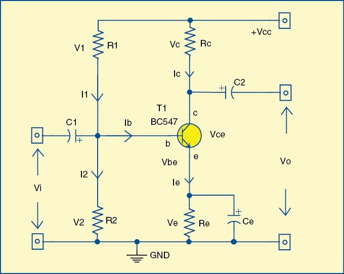
A typical single-stage BJT amplifier consists of:
- Supply voltage VCC
- Collector resistor RC
- Base bias network
- Optional emitter resistor RE
- Coupling capacitors
- Bypass capacitor
Coupling Capacitors
Coupling capacitors isolate the DC bias conditions of each stage while allowing AC signals to pass.
Their impedance is:
Xc = 1 / (2πfC)
At signal frequencies, the impedance is low, allowing signal transmission.
Bypass Capacitors
A bypass capacitor across RE creates two different behaviors:
DC: resistor stabilizes bias
AC: capacitor bypasses the resistor, increasing gain.
Example Calculation for Emitter Stabilization
Assume:
VCC = 12 V
RC = 2 kΩ
RE = 1 kΩ
VB ≈ 2.7 V
VBE ≈ 0.7 V
Emitter voltage:
VE = VB − VBE
VE = 2.7 − 0.7 = 2.0V
Emitter current:
IE = VE / RE
IE = 2.0 V / 1 kΩ = 2 mA
Since:
IC ≈ IE
IC ≈ 2 mA
If temperature increases and IC rises, VE also increases, which reduces VBE and pushes IC downward. This negative feedback stabilizes the operating point.
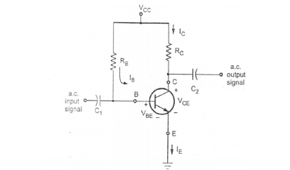
4. Biasing in a Common Emitter Amplifier
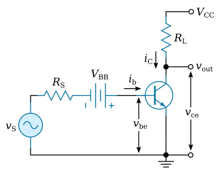
The common emitter amplifier is the most widely used BJT configuration due to:
- High voltage gain
- Moderate input impedance
- Reasonable output impedance
The bias network determines the base current IB, which then controls:
IC = βIB
Where β is transistor DC current gain.
However, β can vary widely due to manufacturing differences and temperature changes. Therefore modern designs avoid bias schemes that depend strongly on β.
Beta-Dependent vs Beta-Independent Bias
| Feature | Beta Dependent | Beta Independent |
|---|---|---|
| Example | Fixed bias | Voltage divider bias |
| Sensitivity to β | High | Low |
| Stability | Poor | Good |
| Q-point variation | Large | Minimal |
5. Major Types of BJT Biasing Circuits
1. Fixed Base Bias
The simplest bias method.
Base current:
IB = (VCC − VBE) / RB
Advantages:
- Simple design
- Low component count
Disadvantages:
- Highly dependent on β
- Poor thermal stability
Common use: switching circuits.
2. Collector Feedback Bias
In this method the base resistor connects to the collector instead of VCC.
If collector current increases:
Vc decreases
Base current decreases
IC reduces
This creates automatic negative feedback.
3. Emitter Feedback Bias
Adding an emitter resistor provides local negative feedback.
If IC increases → VE increases → VBE decreases → IB decreases.
Result: self-correcting bias stabilization.
4. Voltage Divider Bias (Most Common)
Voltage divider bias uses two resistors:
RB1 and RB2
Base voltage:
VB = VCC × (RB2 / (RB1 + RB2))
The divider current is typically designed as:
Idivider ≈ 10IB
When combined with an emitter resistor, the circuit achieves excellent thermal stability.
6. Thermal Runaway Mechanism and Prevention
Thermal runaway occurs when temperature increases cause collector current to increase uncontrollably.
Root Causes
- Increased junction temperature
- Rise in leakage current
- Increase in carrier mobility
- Higher collector current leading to greater power dissipation
The process forms a positive feedback loop:
Temperature ↑ → IC ↑ → Power Dissipation ↑ → Temperature ↑
Effects
- Q-point drift
- Signal distortion
- Device overheating
- Permanent transistor damage
Engineering Prevention Techniques
- Use emitter resistor feedback
- Apply voltage divider bias
- Install heat sinks
- Implement thermal compensation diodes
- Limit power dissipation
- Ensure proper airflow
7. Engineering Applications of Biasing Techniques
| Bias Method | Typical Application |
|---|---|
| Fixed Bias | Digital switching circuits |
| Collector Feedback | Simple amplifier stages |
| Voltage Divider Bias | General analog amplifiers |
| Emitter Bias | Driver stages and power amplifiers |
Voltage divider bias dominates audio amplifiers, sensor amplifiers, and RF pre-stages because of its stability.
8. Advantages and Limitations of Transistor Biasing
Advantages
- Enables linear amplification
- Stabilizes operating point
- Improves thermal reliability
- Reduces sensitivity to transistor variation
- Allows predictable circuit behavior
Limitations
- Requires additional components
- Consumes continuous DC power
- May reduce voltage gain due to feedback
- Requires careful resistor selection
Designing bias networks is therefore a trade-off between stability, gain, and power efficiency.
9. FAQ
1. What is the Q-point in a transistor amplifier?
The Q-point (quiescent point) is the DC operating condition of a transistor when no input signal is present. It defines IC and VCE values and determines the linearity of amplification.
2. Why is transistor bias stability important?
Without stability, temperature changes or transistor gain variation can shift the Q-point, causing distortion, reduced gain, or even device failure.
3. Why is voltage divider bias widely used?
Voltage divider bias sets the base voltage using resistors rather than transistor gain, making the circuit far less sensitive to β variation.
4. What causes thermal runaway in BJTs?
Thermal runaway occurs when rising temperature increases collector current, which further increases power dissipation and heat, forming a positive feedback loop.
5. How can thermal runaway be prevented?
Engineers prevent thermal runaway by using emitter resistors, heat sinks, temperature compensation components, and stable bias networks.
10. Conclusion
Transistor biasing is a critical element in analog electronics that determines whether a circuit behaves predictably or fails under changing conditions. By establishing a stable Q-point and implementing negative feedback through emitter resistors or voltage divider networks, engineers can minimize the impact of temperature variations, transistor gain differences, and supply fluctuations.
Among all biasing techniques, voltage divider bias combined with emitter feedback remains the most widely used solution due to its strong stability and predictable performance. Proper bias design ultimately ensures reliable amplification, improved thermal behavior, and consistent circuit operation.