


64-Pin Ceramic QFN Package: Structure, Materials, Thermal Design, and Engineering Advantages
The 64-pin ceramic QFN (Quad Flat No-Lead) package is a high-reliability semiconductor packaging solution designed for applications requiring superior thermal performance, mechanical stability, and electrical integrity. Compared to plastic QFN, ceramic-based packaging offers improved heat dissipation, lower thermal mismatch, and enhanced environmental resistance. This article provides an engineering-level analysis of its structure, materials, thermal path design, manufacturing process, and real-world application scenarios, helping designers make informed packaging decisions in high-performance systems.
Catalog
- 1. What Is a 64-Pin Ceramic QFN Package
- 2. Package Structure and Internal Architecture
- 3. Ceramic Materials and Thermal Properties
- 4. Key Design Features and Electrical Performance
- 5. Manufacturing Process and Reliability Control
- 6. Ceramic QFN vs Plastic QFN
- 7. Application Scenarios
- 8. Selection Guidelines
- 9. FAQ
- 10. Conclusion
1. What Is a 64-Pin Ceramic QFN Package
A 64-pin ceramic QFN (Quad Flat No-Lead) package is a leadless surface-mount semiconductor package that provides electrical interconnection through bottom-side metallized pads rather than protruding leads. From an engineering perspective, its core value lies in three aspects: thermal efficiency through a direct heat path via the exposed pad, electrical integrity through minimized parasitic inductance, and mechanical reliability due to the inherent stability of ceramic substrates. Compared with traditional leaded packages, QFN significantly reduces loop inductance, making it suitable for RF, high-speed digital, and power semiconductor applications.
2. Package Structure and Internal Architecture
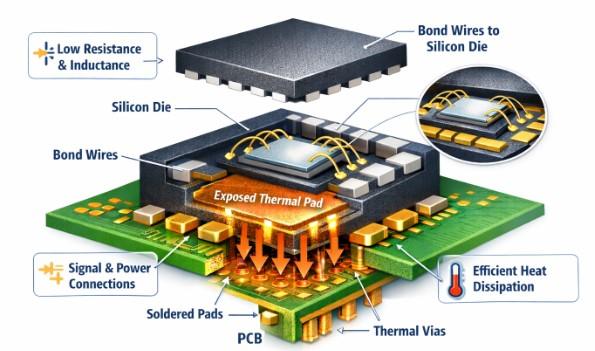
The internal structure of a ceramic QFN is optimized for both thermal conduction and signal integrity. It consists of a multilayer ceramic substrate that provides electrical insulation and mechanical support while enabling compact routing. A semiconductor die is mounted directly onto an exposed thermal pad using a die attach material such as conductive epoxy or solder, which plays a critical role in determining thermal resistance (θJC). Electrical interconnection is achieved through gold or aluminum bond wires connecting the die to metallized pads arranged along the package perimeter.
The exposed thermal pad (EPAD) at the bottom of the package forms the primary heat dissipation path. Heat generated in the die flows vertically through the die attach layer and thermal pad into the PCB, where it is further distributed via copper planes and thermal vias. This direct heat conduction path significantly reduces junction temperature (Tj) and improves overall thermal performance.
3. Ceramic Materials and Thermal Properties
Material selection is a key factor affecting thermal conductivity, coefficient of thermal expansion (CTE), and long-term reliability. Alumina (Al₂O₃) is widely used due to its cost-effectiveness, good electrical insulation, and mature manufacturing process. It offers a thermal conductivity of approximately 20–30 W/m·K, making it suitable for moderate power applications.
Aluminum nitride (AlN), on the other hand, provides significantly higher thermal conductivity in the range of 140–230 W/m·K. Its coefficient of thermal expansion closely matches that of silicon, which reduces thermomechanical stress during temperature cycling. This makes AlN particularly suitable for high-power, high-frequency, and RF applications.
From an engineering standpoint, thermal stress is proportional to the mismatch in CTE between materials and the temperature change. Reducing this mismatch minimizes risks such as die cracking, solder fatigue, and delamination, thereby improving long-term reliability.
4. Key Design Features and Electrical Performance
The leadless architecture of the ceramic QFN package eliminates external leads, thereby reducing parasitic inductance and resistance. This results in improved signal integrity and reduced electromagnetic interference, which is critical in high-frequency applications.
The exposed thermal pad is a central design feature that enhances thermal performance. Proper PCB design is required to fully utilize this advantage, including optimized thermal via placement and adequate copper area for heat spreading. Typical design guidelines include via diameters of 0.2–0.3 mm and via spacing of 0.8–1.2 mm, with filled or tented vias preferred to improve reliability.
The multilayer ceramic substrate enables compact internal routing and supports controlled impedance design, which is essential for RF and high-speed digital circuits. In addition, optional hermetic sealing can be implemented to protect the device from moisture and environmental contamination, making it suitable for aerospace and defense applications.
5. Manufacturing Process and Reliability Control
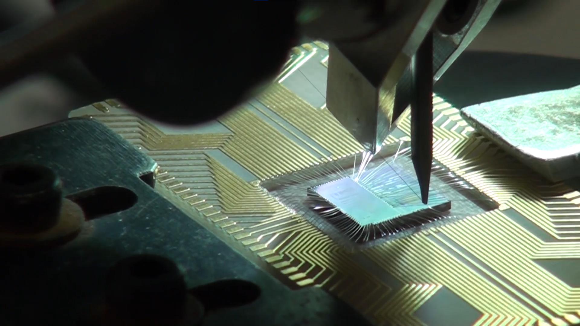
The manufacturing process of ceramic QFN packages begins with ceramic powder preparation, followed by substrate forming and metallization patterning. Multiple layers are stacked and laminated before undergoing high-temperature sintering to achieve structural integrity. After sintering, the semiconductor die is attached to the substrate, and wire bonding is performed to establish electrical connections.
Optional hermetic sealing may be applied using brazing or seam sealing techniques. The package is then finished with nickel/gold (Ni/Au) plating to ensure good solderability and corrosion resistance. Final steps include electrical testing, thermal cycling, and mechanical inspection to ensure compliance with reliability standards.
Critical process controls include maintaining stable sintering conditions to ensure material density, minimizing voids in the die attach layer to optimize thermal performance, and ensuring strong and reliable wire bonds. Reliability testing typically involves thermal cycling, high-temperature storage, hermetic leak testing, and mechanical stress testing.
6. Ceramic QFN vs Plastic QFNe-off
| Parameter | Ceramic QFN | Plastic QFN | Engineering Impact |
|---|---|---|---|
| CTE | 4–7 ppm/°C | 15–25 ppm/°C | Lower stress, higher reliability |
| Thermal Conductivity | High | Moderate | Better heat dissipation |
| Hermeticity | Available | No | Moisture protection |
| Mechanical Stability | Excellent | Moderate | Resists warpage |
| Cost | High | Low | Trade-off: performance vs cost |
Ceramic QFN packages are widely used in high-reliability and high-performance systems. In aerospace and defense, they are applied in avionics, radar systems, and satellite electronics where environmental resistance is critical. In RF and telecommunications, they are used in RF front-end modules and 5G infrastructure due to their excellent high-frequency performance.
In power electronics, ceramic QFN packages are suitable for GaN and SiC devices as well as motor control systems where efficient heat dissipation is required. In medical applications, they are used in implantable devices and imaging systems, where reliability and stability are essential.
8. Selection Guidelines
Ceramic QFN packages should be selected when the application involves high power density, strict thermal management requirements, or operation in harsh environments. They are also ideal for systems requiring high-frequency performance and low parasitic effects.
Designers should evaluate system-level constraints, including thermal budget, mechanical stress, environmental conditions, and lifecycle expectations, before choosing ceramic over plastic packaging.
9. FAQ
Q1: Why use ceramic instead of plastic QFN?
Ceramic materials provide higher thermal conductivity and better CTE matching with silicon, which improves heat dissipation and reduces mechanical stress.
Q2: Is ceramic QFN necessary for all designs?
No, ceramic QFN is typically used in high-performance or high-reliability applications. Plastic QFN is sufficient for most consumer electronics.
Q3: What is the most critical failure point?
Common failure risks include poor soldering of the thermal pad, voids in the die attach layer, and fatigue caused by thermal cycling.
Q4: Is ceramic QFN suitable for RF applications?
Yes, its low parasitic inductance and stable material properties make it highly suitable for RF and high-frequency circuits.
10. Conclusion
The 64-pin ceramic QFN package provides an optimal balance of thermal efficiency, electrical performance, and mechanical reliability. Although it has a higher cost compared to plastic alternatives, its superior performance makes it essential for demanding applications such as aerospace, RF systems, and power electronics. From an engineering perspective, it is a strategic packaging choice that enhances long-term system stability and performance.