


DRAM Performance: A Complete Selection and Optimization Guide for Hardware Engineers
Table of Contents
- Introduction: Why DRAM Performance Matters in Modern System Design
- Key Technical Parameters That Define DRAM Performance
- How to Choose the Right DRAM Configuration for Your Application
- Performance Comparison: DDR4 vs DDR5 vs LPDDR5
- Design Considerations and Common Pitfalls
- Testing and Validation Best Practices
- Frequently Asked Questions
- Conclusion and Next Steps
1. Introduction: Why DRAM Performance Matters in Modern System Design
DRAM performance is a critical bottleneck in modern computing systems, from high-performance servers to automotive ADAS platforms. While processor speeds have increased exponentially, memory bandwidth and latency often determine real-world application performance. Understanding DRAM performance parameters is essential for hardware engineers making component selection decisions that impact system throughput, power consumption, and cost.
This guide provides a technical framework for evaluating DRAM performance across different memory technologies, application scenarios, and design constraints. Whether you're designing a data center server, an embedded vision system, or a high-end gaming platform, this guide will help you make informed decisions about DRAM selection and optimization.
The primary DRAM performance metrics include data transfer rate (MT/s), latency timing (CAS latency, tRCD, tRP), bandwidth utilization, power efficiency, and thermal characteristics. However, real-world performance depends on workload patterns, memory controller efficiency, and system-level factors that datasheet specifications don't fully capture. This guide bridges the gap between theoretical specifications and practical design considerations.
2. Key Technical Parameters That Define DRAM Performance
Understanding DRAM performance requires analyzing multiple interdependent parameters. The most critical specifications that directly impact system performance include data rate, timing parameters, and power characteristics.
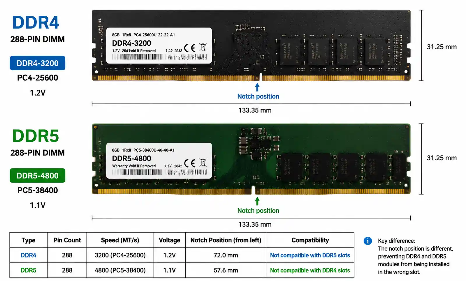
Data Transfer Rate (MT/s) represents the number of memory transfers per second. DDR (Double Data Rate) technology transfers data on both rising and falling clock edges. DDR4 operates at 1600-3200 MT/s, while DDR5 reaches 4800-8400 MT/s. However, higher data rates don't automatically translate to better application performance if latency or command scheduling become bottlenecks.
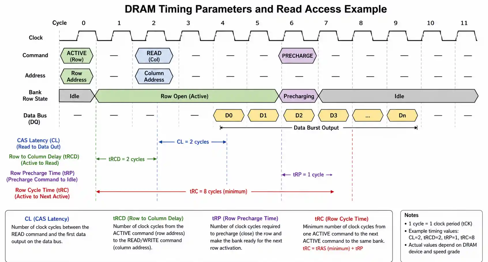
CAS Latency (CL) measures the delay between a read command and data availability. It's specified in clock cycles, not absolute time. A DDR4-3200 module with CL16 has an absolute latency of 10ns (16 cycles / 1600 MHz), while DDR5-4800 with CL40 also has approximately 16.67ns latency. When comparing DRAM technologies, always calculate absolute latency rather than relying solely on CL numbers.
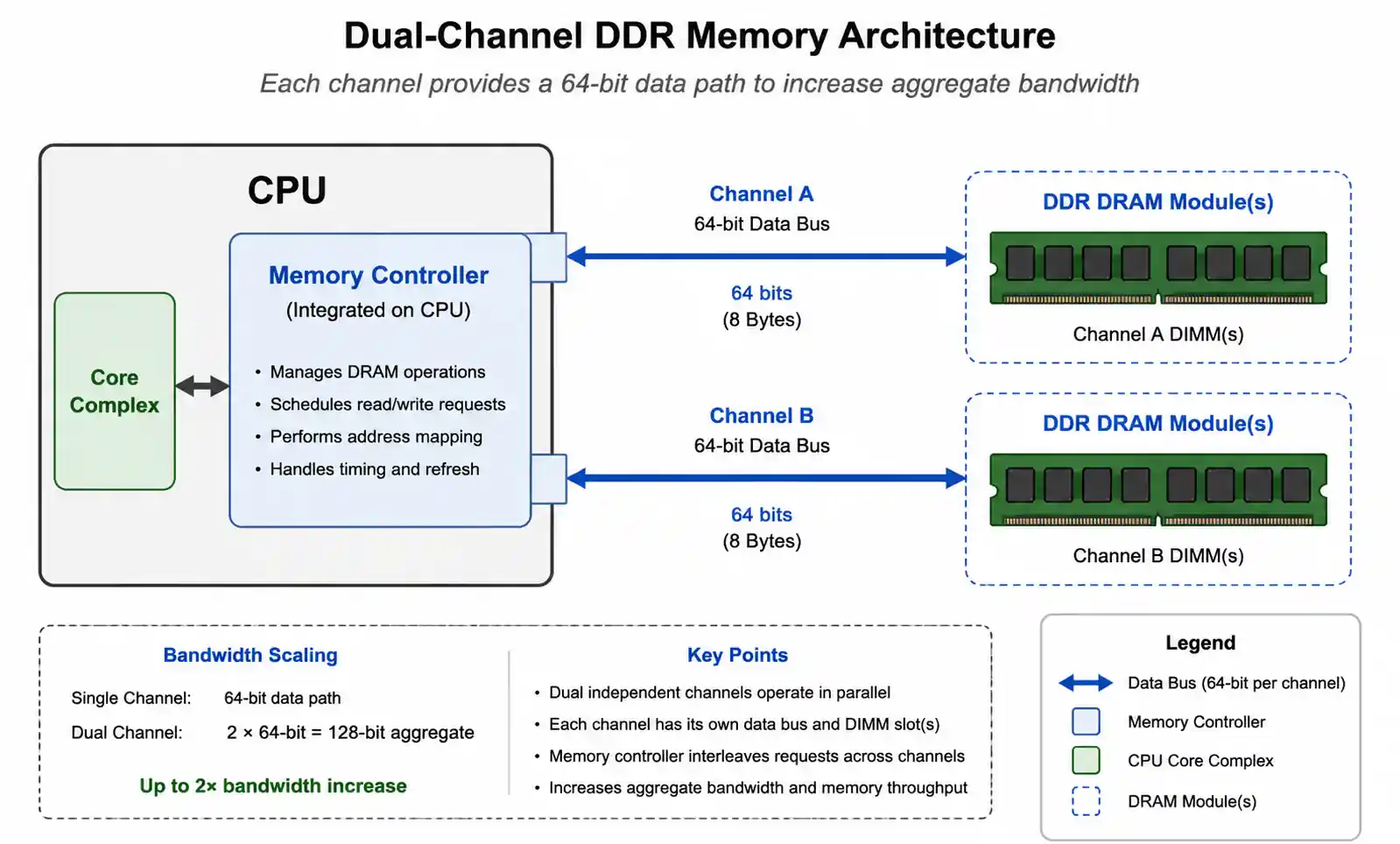
Memory Bandwidth is the theoretical maximum data transfer rate, calculated as: Bandwidth (GB/s) = (Data Rate × Bus Width × Number of Channels) / 8. A dual-channel DDR4-3200 configuration with 64-bit per channel provides 51.2 GB/s theoretical bandwidth. Real-world sustained bandwidth typically reaches 70-85% of theoretical maximum due to refresh cycles, command overhead, and memory controller efficiency.
Row Cycle Time (tRC) determines how quickly the memory can open a new row after closing the previous one. Typical DDR4 tRC ranges from 45-50ns, while DDR5 maintains similar absolute timing despite higher clock speeds. Applications with poor spatial locality that frequently access different memory rows are particularly sensitive to tRC timing.
Refresh Rate impacts effective bandwidth and power consumption. Standard DDR4 refreshes every 64ms across 8192 rows, consuming approximately 5-10% of available bandwidth. DDR5 introduces per-bank refresh to reduce refresh penalty, but higher density modules may require faster refresh rates that impact performance.
3. How to Choose the Right DRAM Configuration for Your Application
DRAM selection should follow a systematic methodology that considers workload characteristics, performance requirements, power budgets, and supply chain constraints.
Step 1: Analyze Memory Access Patterns. Sequential access patterns with high spatial locality benefit most from high bandwidth configurations. Random access patterns with poor locality are latency-sensitive and benefit more from lower CAS latency even at lower data rates. Use memory profiling tools to characterize your application's read/write ratio, burst lengths, and bank utilization before selecting DRAM specifications.
Step 2: Calculate Required Bandwidth. Determine peak and sustained bandwidth requirements. For example, a 4K60 video processing pipeline requires approximately 8-12 GB/s sustained bandwidth considering input, processing buffers, and output. Add 30-40% headroom for system overhead and future expansion. If calculated bandwidth exceeds 80% of theoretical DRAM bandwidth, consider dual-channel or higher-speed memory.
Step 3: Evaluate Latency Requirements. Real-time systems and latency-sensitive applications should prioritize absolute latency over raw bandwidth. For automotive ADAS systems with sub-100ms response requirements, DDR4-2666 with CL15 may outperform DDR4-3200 with CL18 despite lower bandwidth, because the absolute latency is 11.25ns vs 11.25ns.
Step 4: Consider Power Constraints. LPDDR5 consumes 20-30% less power than standard DDR5 at equivalent performance levels, making it essential for battery-powered devices. Server applications should evaluate performance-per-watt metrics, as memory can consume 15-25% of total system power in high-capacity configurations.
Step 5: Assess Thermal Management. High-speed DRAM generates significant heat, particularly in dense multi-rank configurations. DDR5 operating at 6400 MT/s can dissipate 5-8W per module under sustained load. Ensure your PCB design includes adequate thermal vias, ground planes, and airflow for the selected memory configuration.
4. Performance Comparison: DDR4 vs DDR5 vs LPDDR5
The following table compares key performance characteristics across current DRAM technologies:
| Parameter | DDR4-3200 | DDR5-4800 | DDR5-6400 | LPDDR5-6400 |
|---|---|---|---|---|
| Data Rate (MT/s) | 3200 | 4800 | 6400 | 6400 |
| Theoretical Bandwidth (GB/s, dual-channel) | 51.2 | 76.8 | 102.4 | 102.4 |
| Typical CAS Latency | CL16-18 | CL38-40 | CL40-46 | CL40-50 |
| Absolute Latency (ns) | 10-11.25 | 15.8-16.7 | 12.5-14.4 | 12.5-15.6 |
| Operating Voltage (V) | 1.2 | 1.1 | 1.1 | 1.05 |
| Power Consumption (W/module) | 3-5 | 4-7 | 5-8 | 2.5-4.5 |
| Maximum Capacity (GB/module) | 32 | 64 | 64 | 16 (LPDRAM) |
| Bank Groups | 4 | 8 | 8 | 8 |
| Burst Length | 8 | 16 | 16 | 32 |
| Target Application | Desktop, Server | High-performance Server | Enthusiast, HPC | Mobile, Automotive |
This comparison reveals several important trade-offs. DDR5 provides substantially higher bandwidth but at higher absolute latency compared to fast DDR4 configurations. The increased bank groups (8 vs 4) improve parallelism for concurrent memory operations, partially offsetting the latency increase for multi-threaded workloads.
LPDDR5 offers comparable bandwidth to DDR5 while consuming 30-40% less power, but with limited capacity and soldered BGA packaging that eliminates field upgradeability. This makes LPDDR5 ideal for embedded systems where power efficiency outweighs flexibility.
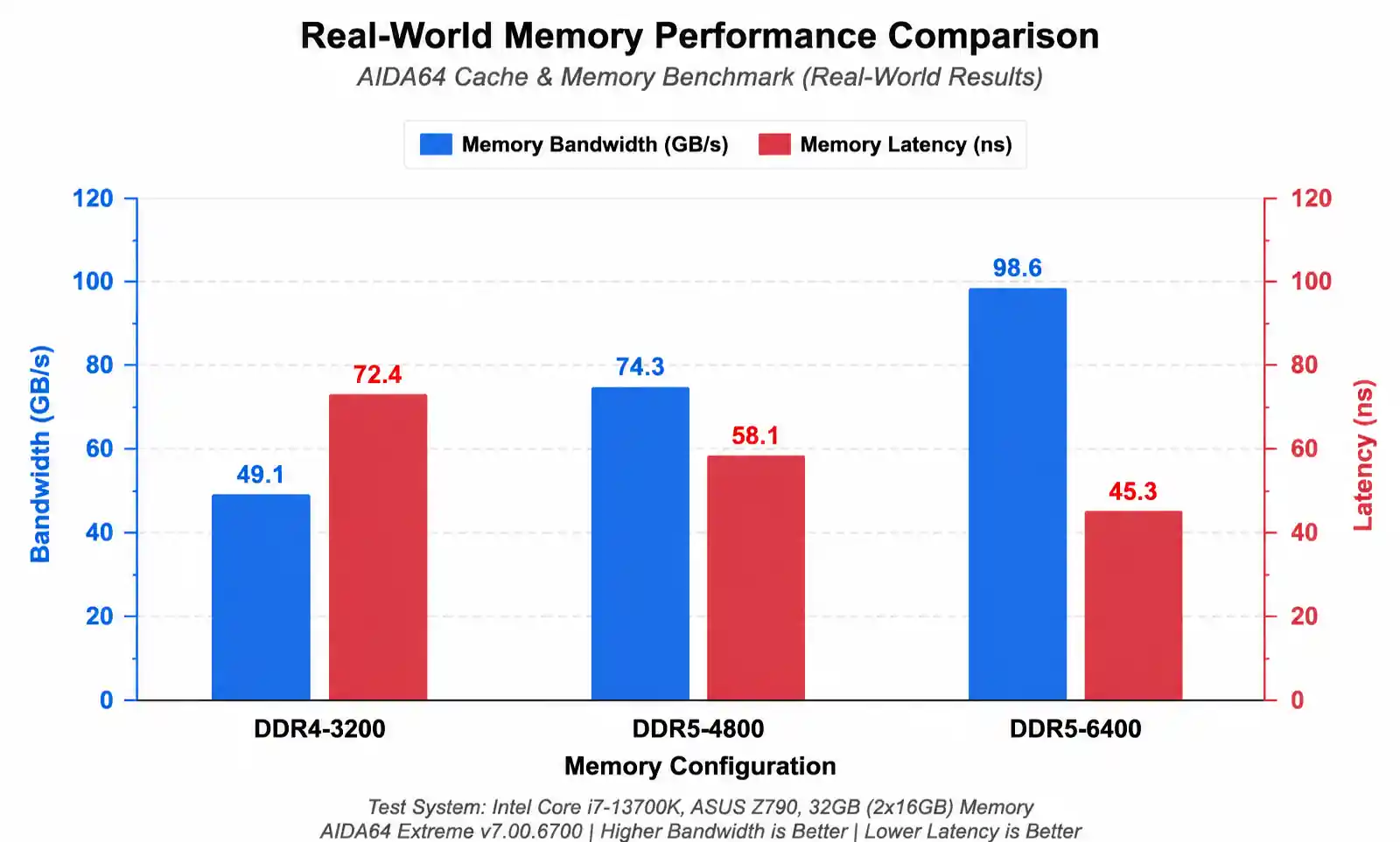
For bandwidth-intensive workloads such as machine learning inference, video encoding, or scientific computing, DDR5-6400 provides 2× the theoretical bandwidth of DDR4-3200. Real-world testing shows sustained bandwidth improvements of 60-80% in memory-bound applications.
For latency-sensitive applications including real-time control systems, high-frequency trading, or gaming, the absolute latency difference between DDR4-3200 CL16 (10ns) and DDR5-4800 CL40 (16.7ns) can impact frame times and response consistency. Some applications may benefit from DDR5-6400 with optimized CL40 timing (12.5ns absolute latency) which offers both improved bandwidth and competitive latency.
5. Design Considerations and Common Pitfalls
Achieving specified DRAM performance requires careful attention to PCB design, signal integrity, power delivery, and thermal management. Common design mistakes can degrade performance by 20-40% or cause system instability.
Signal Integrity and PCB Layout. Memory traces must maintain controlled impedance (typically 40-60 ohms for DDR4/DDR5). Length matching between data, address, and command traces is critical—DDR5 requires ±5ps timing matching for 6400 MT/s operation. Violating these constraints causes signal reflections, eye closure, and increased bit error rates. Always place decoupling capacitors within 3-5mm of DRAM power pins using short, wide traces to minimize inductance.
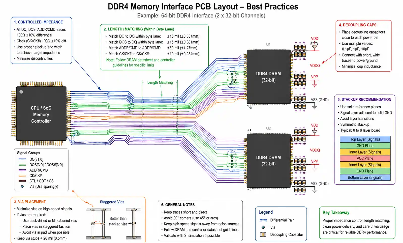
Power Delivery Network Design. DRAM draws significant transient currents during simultaneous switching. A dual-channel DDR5 configuration can draw 20-30A peak current during write bursts. Insufficient decoupling capacitance causes voltage droop that triggers refresh errors or data corruption. Use a combination of bulk capacitors (47-100µF), ceramic capacitors (10µF, 1µF), and high-frequency decoupling capacitors (100nF, 10nF) distributed across the power plane.
Memory Controller Configuration. Default BIOS settings often use conservative timing parameters that sacrifice performance for compatibility. After validating system stability, optimize tRCD, tRP, and command rate settings. Reducing command rate from 2T to 1T can improve bandwidth by 5-10% in applications with high command density. However, aggressive timing with insufficient voltage margin causes intermittent errors that are difficult to diagnose.
Common Mistake: Ignoring Temperature Effects. DRAM timing parameters degrade at elevated temperatures. A module stable at 50°C may experience errors at 85°C if timing margins are too tight. DDR5 includes on-die ECC to mitigate this, but error correction overhead can reduce effective bandwidth by 2-3%. Always validate memory stability across the full operating temperature range, not just at room temperature.
Common Mistake: Overlooking Refresh Overhead. Applications requiring sustained high bandwidth must account for refresh cycles. During refresh, memory cannot service read/write commands. High-density DDR5 modules with 32Gb or larger chips may use higher refresh rates that consume 8-12% of available bandwidth. For real-time applications, consider the impact of refresh cycles on worst-case latency and bandwidth availability.
Supply Chain Considerations. DRAM pricing and availability fluctuate significantly based on market conditions. Design flexibility into your memory subsystem to accept multiple speed grades or qualified second sources. DDR5 adoption has been slower than anticipated, sometimes making high-performance DDR4 more cost-effective for mid-range applications. Always validate your supply chain can support production volumes before finalizing component selection.
6. Testing and Validation Best Practices
Comprehensive DRAM testing must go beyond simple POST checks to validate performance under realistic workloads and environmental conditions.
Memory Stress Testing. Use tools like MemTest86, Prime95, or AIDA64 to stress test memory subsystems for a minimum of 24-48 hours at operating temperature. These tools generate access patterns that expose timing margin issues, thermal throttling, and intermittent errors that may not appear in typical application testing. A system that passes 48 hours of stress testing has approximately 99% confidence of field reliability.
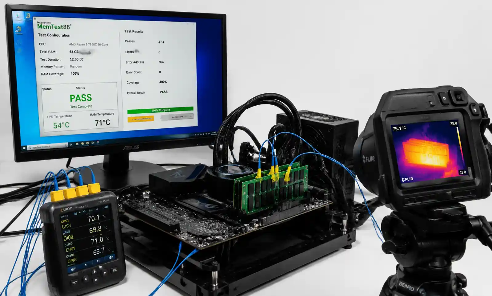
Bandwidth and Latency Benchmarking. Measure actual achieved bandwidth using tools like AIDA64 Memory Benchmark or Intel Memory Latency Checker. Compare results against theoretical specifications. DDR4-3200 should achieve 48-52 GB/s dual-channel bandwidth; significantly lower results indicate configuration issues, thermal throttling, or sub-optimal memory controller settings.
Thermal Validation. Monitor DRAM temperature during sustained workloads using on-die thermal sensors (available in DDR5) or thermal cameras. Memory exceeding 85°C may require improved airflow, heatsinks, or reduced operating frequency. Server applications with high-capacity multi-rank configurations may need active cooling to maintain performance under sustained load.
Signal Integrity Analysis. For production designs, validate eye diagrams and signal quality using an oscilloscope or logic analyzer. DDR5 at 6400 MT/s has approximately 156ps unit interval; maintaining adequate eye opening requires precise impedance control and minimal crosstalk. Signal integrity issues cause correctable errors that degrade performance even if the system remains stable.
The following table outlines recommended validation testing for different application categories:
| Application Type | Minimum Stress Test Duration | Thermal Range | Bandwidth Target | Acceptable Error Rate |
|---|---|---|---|---|
| Consumer Desktop | 24 hours | 25-70°C | >90% theoretical | 0 uncorrectable |
| High-performance Gaming | 48 hours | 25-75°C | >92% theoretical | 0 uncorrectable |
| Industrial/Automotive | 72 hours | -40-105°C | >85% theoretical | 0 errors (including correctable) |
| Server/Data Center | 96 hours | 25-85°C | >88% theoretical | <1 correctable per 10^15 bits |
| Safety-critical Systems | 168 hours | Full operating range | >85% theoretical | 0 errors with margin testing |
After validation testing, document the qualified memory configurations, validated timing parameters, and environmental test results for production reference and field troubleshooting.
7. Frequently Asked Questions
What is the difference between DDR4 and DDR5 in real-world performance?
DDR5 provides 50-100% higher bandwidth compared to DDR4 in memory-bound workloads such as video encoding, large dataset processing, and scientific computing. However, absolute latency is 30-50% higher in comparable DDR5 configurations, which can impact latency-sensitive applications. DDR5's improved bank interleaving and on-die ECC provide better sustained performance under heavy multi-threaded workloads. For most applications, DDR5-5600 or higher provides measurable performance improvements; DDR5-4800 may not justify the cost premium over fast DDR4.
How do I calculate the actual latency of DRAM in nanoseconds?
Absolute latency (ns) = (CAS Latency × 2000) / Data Rate (MT/s). For example, DDR4-3200 CL16 has (16 × 2000) / 3200 = 10ns latency. DDR5-4800 CL40 has (40 × 2000) / 4800 = 16.67ns latency. Always compare absolute latency when evaluating different DRAM technologies, not just CAS latency numbers.
Can I mix different DRAM speeds or capacities in a dual-channel configuration?
Mixing DRAM modules is generally not recommended. If different capacity modules are used, the system typically operates in flex mode with reduced performance. If different speed grades are mixed, all modules run at the lowest common speed. Mixing manufacturers or chip configurations can cause stability issues due to varying electrical characteristics. For optimal performance and reliability, use identical modules in all memory channels.
What memory speed do I actually need for my application?
This depends on your workload. CPU-bound applications with small working sets show minimal benefit from faster memory. Memory-bound applications (video editing, 3D rendering, large-scale simulations) benefit significantly from higher bandwidth. Gaming typically shows 5-15% performance improvement from DDR4-3200 to DDR4-3600, with diminishing returns beyond 4000 MT/s. Profile your application to identify if memory bandwidth or latency is the bottleneck before investing in premium memory.
How important is CAS latency compared to memory speed?
Both matter, but their importance varies by workload. Sequential memory access patterns benefit more from high bandwidth (higher MT/s), while random access patterns benefit more from low latency (lower CL). The absolute latency formula shows that DDR4-3600 CL18 (10ns) and DDR4-3200 CL16 (10ns) have identical latency but different bandwidth. For most mixed workloads, balanced configurations (e.g., DDR4-3600 CL16 or DDR5-6000 CL36) provide optimal price-performance.
What are the main causes of DRAM performance degradation over time?
DRAM performance typically remains stable, but system-level factors can cause apparent degradation. Thermal interface material aging increases operating temperature, forcing thermal throttling or timing relaxation. Accumulated dust reduces airflow and increases temperature. Memory controller driver updates may change default timing parameters. Increased background processes or OS overhead can reduce available bandwidth. True DRAM cell degradation is rare but can occur in high-temperature environments or with improper voltages.
Do I need ECC memory for my application?
ECC (Error-Correcting Code) memory is essential for servers, data centers, scientific computing, and any application where data integrity is critical. ECC detects and corrects single-bit errors automatically, preventing data corruption. Consumer platforms typically don't support ECC, but workstation and server platforms require it. DDR5 includes on-die ECC as standard, which improves reliability even in non-ECC systems, though it doesn't provide system-level error reporting like true ECC modules.
How do I optimize memory performance in BIOS/UEFI settings?
Start by enabling XMP (Intel) or DOCP/EXPO (AMD) profiles to run memory at rated speeds rather than default JEDEC specifications. Advanced users can manually tune primary timings (CL, tRCD, tRP, tRAS) and secondary timings (tRFC, tRRD, tWR) for improved performance. Reduce command rate from 2T to 1T if stable. Increase DRAM voltage slightly (1.35V-1.4V for DDR4) to improve timing margins. Always stress test for 24+ hours after timing changes to ensure stability.
8. Conclusion and Next Steps
Picking DRAM is always a trade‑off: bandwidth, latency, power, and cost. DDR5 wins for memory‑hungry workloads, DDR4 still holds its own for latency‑sensitive tasks, and LPDDR5 is the go‑to for battery‑powered gear.For HPC or data center, aim for DDR5‑5600 or faster, tweak timings, and don't skimp on cooling. For real‑time embedded, focus on absolute latency and thermal stability across your temperature range. On a budget? DDR4‑3200 CL16 gives you great bang for the buck.
Before you lock in your choice, test with your actual workload, stress the system, and verify signal integrity on your PCB. Grab the datasheets and layout notes from the vendor. And if you're unsure, ping the FAE team or use their online configurator—they can save you from expensive mistakes.