


How CMOS Image Sensors Work in Cameras: Architecture, Signal Chain, and Selection Guide
CMOS image sensors are the dominant imaging technology in modern electronics, enabling devices to convert optical signals into digital images efficiently. This article provides a technical breakdown of CMOS sensor architecture, pixel operation, signal readout, performance trade-offs, and selection criteria. It also compares CMOS with CCD sensors from an engineering perspective to support design and procurement decisions.
Table of Contents
- 1. What Is a CMOS Image Sensor?
- 2. CMOS Sensor Architecture and Pixel Structure
- 3. CMOS Image Sensor Working Principle
- 4. Readout Mechanisms: Rolling vs Global Shutter
- 5. Performance Characteristics and Trade-offs
- 6. Advantages and Limitations
- 7. Application Scenarios
- 8. CMOS Sensor Selection Guide
- 9. CMOS vs CCD: Engineering Comparison
- 10. Conclusion
- FAQ
1. What Is a CMOS Image Sensor?
A CMOS (Complementary Metal-Oxide-Semiconductor) image sensor is a semiconductor device that converts incident light into digital signals using an array of photodiodes and integrated readout circuitry.
Unlike early imaging technologies, CMOS sensors integrate amplification, noise reduction, and analog-to-digital conversion directly on-chip. This system-on-chip architecture significantly reduces system complexity, power consumption, and cost.
At a structural level, a CMOS sensor consists of:
- Pixel array (photodiodes + transistors)
- Row/column selection circuits
- Analog front-end (AFE)
- ADC (Analog-to-Digital Converter)
- Digital processing logic
2. CMOS Sensor Architecture and Pixel Structure
![]()
2.1 Active Pixel Sensor (APS) Concept
Modern CMOS sensors use Active Pixel Sensor (APS) architecture. Each pixel includes:
- Photodiode (light detection)
- Reset transistor
- Source follower amplifier
- Row select transistor
This enables per-pixel amplification, reducing noise and improving readout speed.
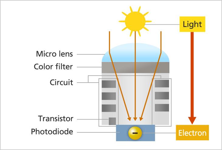
2.2 Pixel Stack
A typical pixel includes:
- Microlens (focus light)
- Color filter (RGB Bayer pattern)
- Photodiode (charge generation)
- CMOS circuitry (signal conversion)
2.3 Fill Factor
Fill factor defines the percentage of pixel area sensitive to light. Higher fill factor improves sensitivity, especially in low-light conditions.
3. CMOS Image Sensor Working Principle
3.1 Photoelectric Conversion
Incoming photons strike the photodiode:
- Generate electron-hole pairs
- Accumulate charge proportional to light intensity
3.2 Charge-to-Voltage Conversion
Each pixel converts accumulated charge into a voltage signal via its internal amplifier.
3.3 Row-by-Row Readout
Pixels are accessed sequentially:
- Row select activates a line
- Column circuits read voltage values
- Signals are passed to ADC
3.4 Analog-to-Digital Conversion
The analog voltage is digitized into pixel values, forming a raw image.
3.5 Image Processing Pipeline
Post-processing includes:
- Demosaicing (Bayer interpolation)
- Noise reduction
- White balance
- Gamma correction
4. Readout Mechanisms: Rolling vs Global Shutter
4.1 Rolling Shutter
- Reads pixels line-by-line
- Lower cost and power
- Causes distortion (skew, wobble) in fast motion
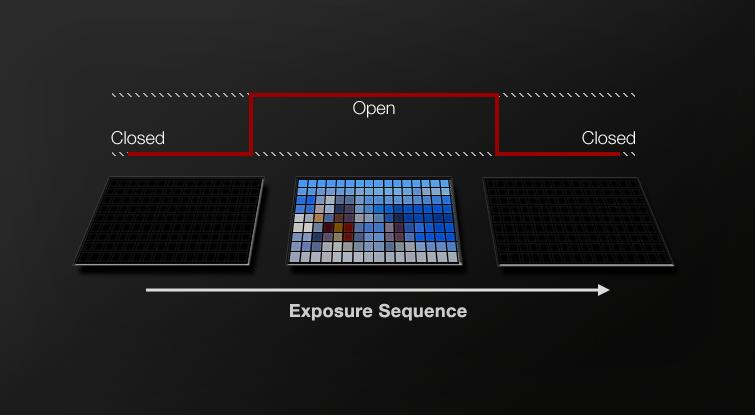
4.2 Global Shutter
- Captures all pixels simultaneously
- Eliminates motion artifacts
- Requires more complex pixel design (lower fill factor)
5. Performance Characteristics and Trade-offs
5.1 Key Parameters
- Resolution (MP) – spatial detail
- Pixel Size (µm) – light sensitivity
- Dynamic Range (dB) – bright/dark detail
- Signal-to-Noise Ratio (SNR) – image clarity
- Quantum Efficiency (QE) – photon conversion efficiency
5.2 Trade-off Example
- Smaller pixels → higher resolution but more noise
- Larger pixels → better low-light but lower density
6. Advantages and Limitations
Advantages
- Low power consumption (ideal for mobile devices)
- High integration (SoC architecture)
- Fast readout (high FPS support)
- Cost-effective fabrication (standard CMOS process)
Limitations
- Rolling shutter distortion
- Noise in low-light (especially small pixels)
- Fixed pattern noise (FPN)
- Thermal sensitivity
7. Application Scenarios
Consumer Electronics
- Smartphones
- Digital cameras
- Webcams
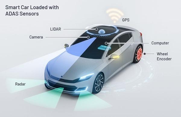
Automotive
- ADAS (lane detection, object recognition)
- Rear-view and surround cameras
Industrial Vision
- Quality inspection
- Robotics guidance
Medical Imaging
- Endoscopy
- Diagnostic imaging systems
8. CMOS Sensor Selection Guide
8.1 Resolution vs Application
- Surveillance → 2–8 MP
- Industrial inspection → high resolution
- Mobile → balance resolution and power
8.2 Pixel Size
- ≥1.4 µm → better low-light
- <1.0 µm → compact, high-density
8.3 Shutter Type
- Rolling → general use
- Global → motion-critical applications
8.4 Frame Rate
- ≥60 FPS for motion capture
- ≥120 FPS for high-speed imaging
8.5 Power Consumption
Critical for:
- Battery devices
- Embedded systems
9. CMOS vs CCD: Engineering Comparison
| Parameter | CMOS Sensor | CCD Sensor |
|---|---|---|
| Readout Method | Parallel pixel readout | Serial charge transfer |
| Power Consumption | Low | High |
| Speed | High | Lower |
| Integration | High (ADC on-chip) | Low |
| Noise | Moderate (modern: low) | Very low |
| Cost | Low | High |
| Applications | Consumer, automotive | Scientific imaging |
10. Conclusion
CMOS image sensors dominate modern imaging systems due to their integration capability, low power consumption, and scalability. Their architecture enables efficient signal processing directly on-chip, making them suitable for everything from smartphones to industrial vision systems. Understanding pixel design, readout methods, and performance trade-offs is essential for selecting the right sensor in engineering applications.
FAQ
Q1: Why are CMOS sensors more popular than CCD today?
Because they offer lower power consumption, faster readout, and easier integration with digital circuits.
Q2: What causes rolling shutter distortion?
Sequential row readout causes time delay across the image, leading to skew in moving objects.
Q3: Are CMOS sensors suitable for low-light imaging?
Yes, especially modern sensors with larger pixels and backside illumination (BSI).
Q4: What is the role of ADC in CMOS sensors?
It converts analog pixel signals into digital values for image processing.
Q5: How do I choose between global and rolling shutter?
Use global shutter for motion accuracy; use rolling shutter for cost-sensitive applications.