


SiC Packaging: A Practical Guide to Power Module Design and Material Selection
Silicon carbide has moved from research labs into production lines faster than most predicted. But here's what design teams often miss: the semiconductor die is only half the story. The packaging around that SiC chip determines whether your power module hits its thermal targets, survives automotive qualification, or fails in the field after six months.
This guide walks through the key decisions in SiC packaging—from substrate materials and die attach to thermal interfaces and encapsulation—based on what actually matters in high-power, high-temperature applications. We'll cover the trade-offs that datasheets don't always spell out and the design choices that separate reliable modules from warranty nightmares.
Table of Contents
- What Makes SiC Packaging Different from Silicon
- Critical Packaging Materials and Their Thermal Limits
- Substrate Selection: DBC, AMB, and Direct Bond Aluminum
- Die Attach Technologies for High-Temperature Operation
- Thermal Management Strategies in SiC Power Modules
- Reliability Challenges and Failure Modes
- FAQ
- Conclusion
1. What Makes SiC Packaging Different from Silicon
Silicon carbide dies operate at junction temperatures that would destroy conventional silicon IGBTs. While a silicon device might be rated to 150°C junction temperature, SiC MOSFETs routinely run at 175°C and can handle transient spikes above 200°C. This capability is valuable—higher operating temperatures mean smaller heatsinks and better power density—but it creates challenges that standard packaging wasn't designed to handle.
The mismatch in coefficient of thermal expansion (CTE) becomes critical. A SiC die has a CTE around 4.2 ppm/°C, while traditional packaging materials like FR-4 substrates or standard solder alloys have CTEs two to five times higher. Every thermal cycle—startup, load change, shutdown—creates mechanical stress at the interfaces. Over thousands of cycles in automotive or industrial applications, these stresses cause delamination, solder fatigue, or wire bond liftoff.
Switching frequency is the other major difference. SiC devices switch at 20 kHz to 100 kHz or higher, compared to 5-20 kHz for silicon IGBTs. Faster switching reduces losses but creates higher di/dt and dv/dt, which places stricter requirements on parasitic inductance. Packaging layout, bond wire length, and internal bus bar design directly affect switching performance. A poorly designed package can negate the switching advantages that made you choose SiC in the first place.
2. Critical Packaging Materials and Their Thermal Limits
Choosing packaging materials for SiC means checking two things: maximum operating temperature and CTE compatibility. Most legacy power module materials were designed for 125-150°C operation. SiC requires materials that remain stable at 175°C continuous and can survive 200°C+ transients without degradation.
| Material | Max Continuous Temp (°C) | CTE (ppm/°C) | Thermal Conductivity (W/m·K) | Typical Use |
|---|---|---|---|---|
| AlN substrate | 250 | 4.5 | 170-180 | High-power modules, close CTE match to SiC |
| Al₂O₃ (96% alumina) | 200 | 6.8 | 20-25 | Cost-effective, moderate thermal performance |
| Si₃N₄ substrate | 250 | 3.2 | 85-90 | High reliability, excellent CTE match |
| Sintered silver die attach | 300 | 19.7 | 240-250 | High-temp die bonding, superior to solder |
| SAC305 solder | 150 | 21.0 | 60 | Standard lead-free, limited to lower-temp SiC |
| Silicone gel encapsulant | 200 | 300 | 0.2 | Wire bond protection, stress relief |
This table shows why aluminum nitride (AlN) has become the substrate of choice for high-performance SiC modules. The CTE is close to SiC itself, and thermal conductivity is an order of magnitude better than alumina. Silicon nitride offers even better CTE matching and excellent mechanical strength, though it costs more and has lower thermal conductivity than AlN.
Die attach is where many first-generation SiC modules ran into trouble. Traditional high-lead or SAC solder alloys begin to creep and fatigue at temperatures above 150°C. Sintered silver die attach, developed initially for high-reliability applications, has become the standard for SiC. It's stable to 300°C, has excellent thermal conductivity, and survives thermal cycling far better than solder. The downside is process complexity and the need for pressure during sintering, but for automotive-grade and industrial SiC modules, it's increasingly non-negotiable.
3. Substrate Selection: DBC, AMB, and Direct Bond Aluminum
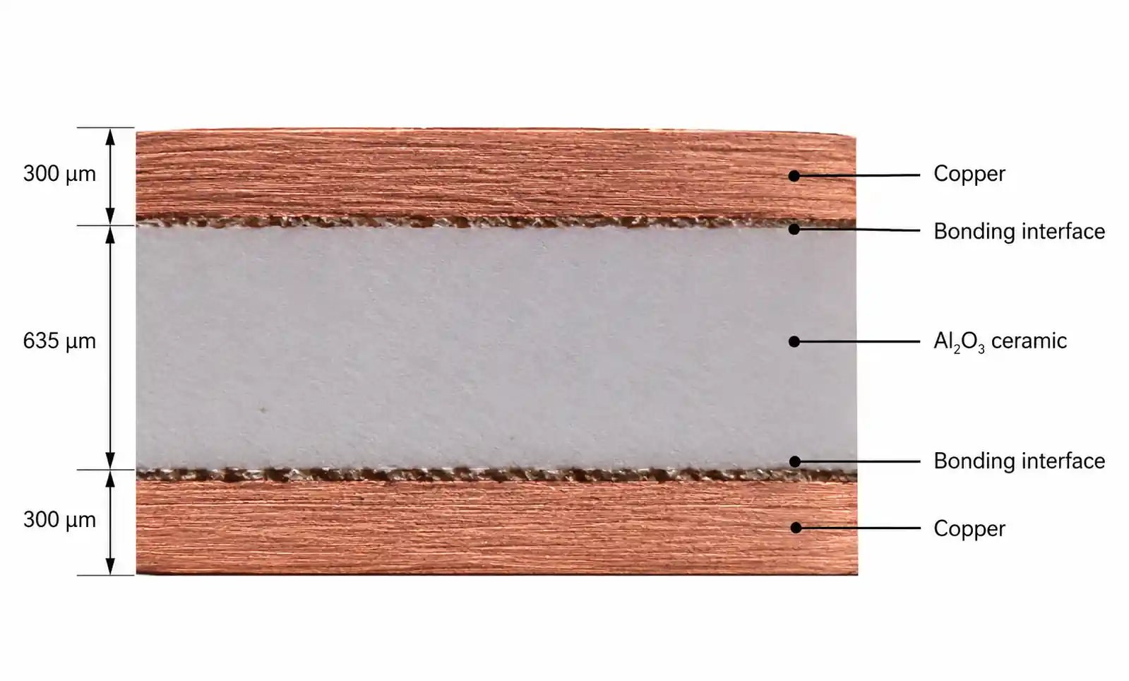
The substrate is the mechanical and thermal backbone of the power module. It provides electrical isolation between the power circuit and the heatsink while conducting heat away from the die. Three technologies dominate in SiC packaging: direct bonded copper (DBC), active metal brazing (AMB), and direct bonded aluminum (DBA).
DBC substrates use a eutectic bonding process to attach copper layers to a ceramic (typically Al₂O₃ or AlN). The copper provides electrical conductivity and helps spread heat, while the ceramic offers dielectric strength and a thermal path to the baseplate. DBC on alumina is cost-effective and works for moderate-power SiC designs where junction temperature stays below 150°C. For higher-power applications, DBC on AlN delivers better thermal performance and reduces the temperature drop across the substrate.
AMB substrates use an active metal brazing layer to bond copper to ceramic, allowing the use of materials like silicon nitride (Si₃N₄) that don't bond well with standard DBC processes. Si₃N₄ substrates offer outstanding mechanical strength and thermal shock resistance, making them suitable for applications with severe thermal cycling—think traction inverters or industrial motor drives where load transients are frequent and large. The CTE of Si₃N₄ is nearly a perfect match for SiC, which translates into longer die attach life and better long-term reliability.
DBA substrates replace copper with aluminum, which has a CTE closer to ceramic materials and a lower mass. The lower CTE mismatch reduces thermal cycling stress, and the lighter weight can be an advantage in aerospace or high-vibration environments. However, aluminum has lower thermal and electrical conductivity than copper, so DBA is typically used in lower-current designs or where weight and CTE matching are more critical than raw thermal performance.
| Substrate Type | Ceramic | Metal | CTE (ppm/°C) | Thermal Conductivity (W/m·K) | Best For | |---|---|---|---|---| | DBC on Al₂O₃ | Alumina | Copper | 6.8 (ceramic) | ~20 | Cost-sensitive, moderate power | | DBC on AlN | Aluminum Nitride | Copper | 4.5 (ceramic) | 170-180 | High power, better thermal | | AMB on Si₃N₄ | Silicon Nitride | Copper | 3.2 (ceramic) | 85-90 | High reliability, thermal cycling | | DBA | Al₂O₃ or AlN | Aluminum | Variable | Lower than DBC | Weight-sensitive, lower current |
When selecting a substrate, the key trade-off is usually thermal performance versus reliability under thermal cycling. DBC on AlN gives you the best heat spreading and lowest thermal resistance, but if your application sees thousands of power cycles with large temperature swings—typical in automotive traction inverters—the CTE mismatch between copper and ceramic can still cause long-term issues. AMB on Si₃N₄ sacrifices some thermal conductivity but offers better mechanical stability over the module's lifetime.
4. Die Attach Technologies for High-Temperature Operation
Die attach is often the first point of failure in a SiC power module. The interface between the die and substrate must conduct heat, provide electrical connection (in some designs), and survive repeated thermal expansion and contraction without cracking or delaminating. Traditional solder-based die attach begins to fail when junction temperatures regularly exceed 150°C, which is well within the operating range of SiC devices.
Sintered silver has emerged as the leading die attach technology for SiC. The sintering process uses silver particles and pressure (typically 5-40 MPa) at temperatures between 250-300°C to create a solid silver layer with minimal voids. Once sintered, the joint is stable to 300°C or higher, well above any realistic SiC operating temperature. Thermal conductivity is excellent—240 W/m·K or better—and the material doesn't undergo phase transitions that cause fatigue in solder joints.
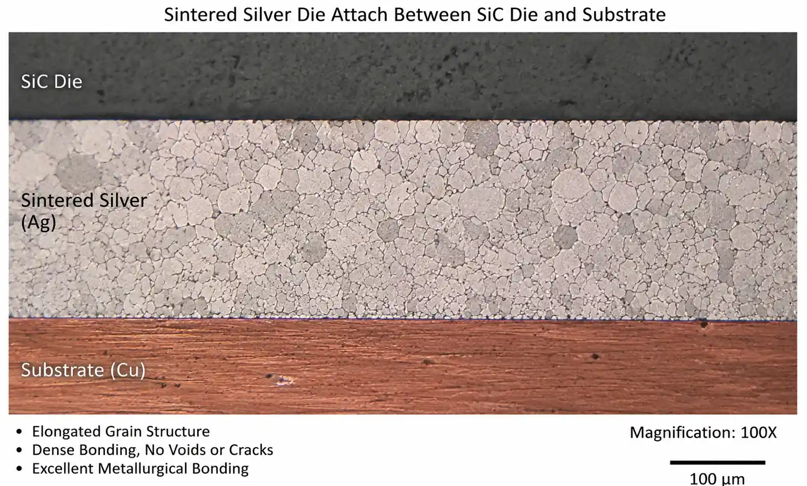
The challenge with sintered silver is process control. Pressure must be applied during sintering, which complicates automation and requires fixtures to hold dies in position. Void content must be kept below 5% for high-reliability applications; voids increase thermal resistance and create stress concentration points. Some vendors have developed pressure-less sintering processes using specialized silver pastes, though these typically require longer process times or higher temperatures.
High-temperature solders—such as AuSn (eutectic at 280°C) or AuGe—are sometimes used as an alternative to sintered silver. These alloys remain solid well above typical SiC operating temperatures and avoid the pressure requirement of sintering. However, gold-based solders are expensive, and the intermetallic compounds formed during soldering can be brittle. They're more common in low-volume or specialized applications where the cost premium is acceptable.
For engineers designing SiC modules today, the decision tree is relatively straightforward. If your application requires automotive-grade reliability (AEC-Q101 qualification) or continuous operation above 150°C junction temperature, plan for sintered silver. If cost is the primary driver and your thermal design keeps junction temperatures below 140°C under worst-case conditions, SAC305 or similar lead-free solders can still work—but expect to see reduced cycle life compared to sintered silver.
5. Thermal Management Strategies in SiC Power Modules
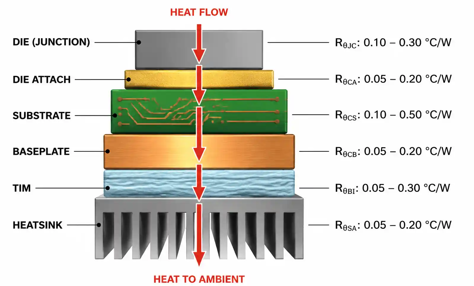
SiC devices can operate at higher temperatures than silicon, but that doesn't mean you should let them. Junction temperature directly affects long-term reliability: every 10°C increase in average operating temperature roughly doubles the failure rate due to acceleration of thermomechanical fatigue and diffusion processes. Effective thermal management in SiC packaging focuses on minimizing thermal resistance from junction to ambient and managing transient thermal loads during switching.
Thermal resistance in a power module is a series of interfaces: die to substrate, substrate to baseplate, and baseplate to heatsink. Each interface adds resistance. A typical SiC module might have a junction-to-case thermal resistance (R_θJC) of 0.2-0.5 K/W, depending on die size and substrate material. The case-to-sink interface, dominated by thermal interface material (TIM), often adds another 0.05-0.15 K/W per square centimeter. Minimizing these resistances means choosing materials carefully and controlling interface quality during assembly.
| Thermal Interface | Material | Thermal Resistance (K/W per cm²) | Max Temp (°C) | Notes | |---|---|---|---| | Die attach (sintered Ag) | Silver | 0.01-0.03 | 300 | Low resistance, high reliability | | Die attach (SAC305) | Tin-silver-copper | 0.03-0.05 | 150 | Adequate for lower-temp designs | | Substrate (AlN DBC) | AlN + copper | 0.08-0.12 | 250 | Excellent thermal conductivity | | TIM (thermal grease) | Silicone compound | 0.10-0.20 | 150-200 | Easy to apply, requires pressure | | TIM (phase change) | Polymer/wax | 0.05-0.10 | 125-150 | Good for automated assembly | | TIM (graphite pad) | Graphite | 0.08-0.15 | 200+ | High temp, moderate performance |
Baseplate design also matters more than many designers assume. Thick copper baseplates (3-5 mm) provide good thermal spreading and mechanical stiffness but add weight and cost. Some newer designs use aluminum baseplates with copper inserts directly under the die locations, balancing thermal performance with weight reduction. In applications where weight is critical—aerospace or high-performance automotive—baseplateless designs bond the substrate directly to a heatsink or cooling plate, eliminating one thermal interface entirely.
Transient thermal management is equally important. During hard switching events, localized heating can create temperature spikes that stress the die attach and wire bonds even if average junction temperature is acceptable. This is where the thermal mass of the substrate comes into play. AlN substrates, despite their excellent thermal conductivity, have lower thermal capacitance than alumina. For applications with high peak power transients, a thicker substrate or a two-layer substrate design can absorb transient heat and reduce peak temperatures.
6. Reliability Challenges and Failure Modes
SiC power modules fail for predictable reasons, and most failures trace back to packaging choices made early in the design. Understanding the common failure modes helps you design them out from the start.
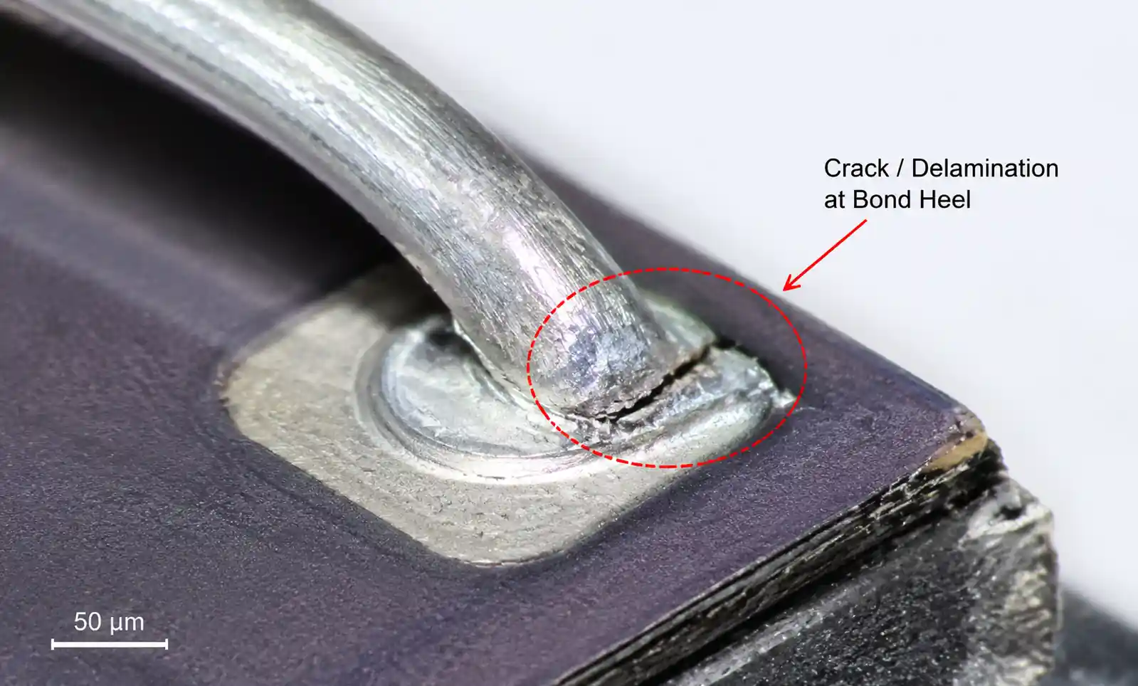
Wire bond fatigue is the most frequent failure mechanism in high-power SiC modules. Aluminum wire bonds—still the most common interconnect technology—undergo repeated thermal expansion and contraction with every load cycle. The bond heel, where the wire attaches to the die, experiences the highest stress concentration. After 50,000 to 200,000 thermal cycles, depending on temperature swing and current density, the wire can crack or lift off entirely. Once a single wire fails, current redistributes to the remaining wires, accelerating fatigue in those bonds until the module fails completely.
Switching to heavier wire (300-500 µm diameter), adding redundant bonds, or moving to ribbon bonds can extend wire bond life. Some high-reliability designs use sintered silver ribbon bonds or even eliminate wire bonds altogether by using top-side metal interconnects. These approaches add cost but can be necessary in automotive traction inverters or industrial drives where the expected lifetime is 15-20 years.
Die attach delamination is the second major failure mode, particularly in modules using solder-based die attach at high operating temperatures. Thermal cycling creates shear stress at the die-substrate interface. If voids are present in the die attach or if the joint temperature regularly exceeds the solder's creep temperature, cracks initiate and propagate. Delamination increases thermal resistance, which raises junction temperature, which accelerates further delamination—a positive feedback loop that leads to thermal runaway.
Preventing die attach failure comes down to material selection (sintered silver for high-temp applications), process control (minimizing voids, ensuring uniform bond line thickness), and thermal design (keeping peak temperatures below material limits). Non-destructive inspection techniques like scanning acoustic microscopy (SAM) can detect voids and delamination before modules ship, but they add cost and cycle time.
Encapsulation cracking is less common but worth considering in designs that see large thermal gradients or high-vibration environments. Silicone gels are the standard encapsulation material for SiC modules because they remain flexible across a wide temperature range and provide stress relief. However, if the module experiences thermal shock—rapid cooling from near-maximum operating temperature—the differential contraction between the gel, the substrate, and the die can create cracks. Once cracked, the encapsulant loses its moisture protection, and corrosion can begin.
7. FAQ
What is the typical lifespan of a SiC power module in automotive applications?
Automotive-grade SiC modules are typically designed to survive 15 years or 150,000 miles under normal operating conditions. This translates to roughly 200,000-500,000 thermal cycles depending on the drive cycle. Actual lifespan depends heavily on average junction temperature and the magnitude of thermal swings during operation. Keeping average Tj below 150°C with sintered silver die attach and proper thermal management typically meets or exceeds this target.
Can I use standard silicon IGBT packaging designs for SiC MOSFETs?
Not for high-temperature or high-reliability applications. Standard IGBT packaging—especially older designs using solder die attach and alumina substrates—will experience accelerated aging when used with SiC devices operating above 150°C junction temperature. The CTE mismatch and thermal cycling stress become critical. For SiC, plan for AlN or Si₃N₄ substrates, sintered silver die attach, and careful attention to wire bond design.
How do I calculate the required thermal resistance for my application?
Start with maximum allowable junction temperature (typically 175°C for SiC MOSFETs), subtract the maximum ambient temperature in your application, then divide by the total power dissipation. That gives you the total allowable thermal resistance from junction to ambient. Subtract the junction-to-case resistance (from the module datasheet) and the case-to-sink interface resistance (typically 0.05-0.15 K/W per cm² depending on TIM). What's left is the maximum heatsink thermal resistance you can tolerate.
What are the key parameters to check in a SiC module datasheet for thermal performance?
Focus on R_θJC (junction-to-case thermal resistance), maximum junction temperature, and thermal cycling capability if provided. Also check die attach technology and substrate material, though not all datasheets specify these. Look for power cycling test results—modules qualified to ECPE or AQG324 standards have undergone standardized thermal cycling tests that give you a realistic picture of reliability.
Is sintered silver die attach always necessary for SiC packaging?
Not always. If your design keeps junction temperature below 150°C under all conditions and you're not targeting automotive or high-reliability industrial markets, SAC305 solder can work. But if you expect junction temperatures in the 150-175°C range, thermal cycling over 100,000 cycles, or need to meet AEC-Q101 qualification, sintered silver is the safer choice. The process cost premium has narrowed as sintering equipment and materials have matured.
What causes parasitic inductance in SiC modules and how can I minimize it?
Parasitic inductance comes from the current path geometry—wire bond length, internal bus bar layout, and lead frame design. Longer current paths mean higher inductance. To minimize it, use ribbon bonds or multi-chip parallel configurations instead of single wires, keep internal conductor paths short and wide, and consider kelvin source connections for gate drive circuits. Some advanced modules use embedded die configurations or 3D packaging to reduce loop inductance below 10 nH.
How do I handle thermal interface material degradation over time?
Thermal grease can pump out or dry out after hundreds of thermal cycles, increasing thermal resistance. For long-life applications, consider phase-change materials or graphite pads that maintain stable performance over the module's lifetime. If using thermal grease, factor in a 20-30% increase in thermal resistance over time in your thermal calculations. Some designs use a thin foil of indium or other soft metal as TIM, which conforms to surface roughness and doesn't degrade.
What testing is required to validate SiC module reliability?
At minimum, perform power cycling tests per ECPE recommendations or AQG324 standards, which subject modules to controlled thermal cycles until failure or a defined cycle count (typically 100k-500k cycles). Also conduct thermal shock testing (rapid temperature transitions), high-temperature storage life testing, and humidity-temperature cycling. For automotive applications, vibration and mechanical shock tests per AEC-Q101 are required. These tests are time-consuming but necessary to catch packaging failures before production.
8. Conclusion
SiC packaging isn't just about finding materials that survive high temperatures—it's about managing the entire thermal-mechanical-electrical system to deliver reliable performance over the module's lifetime. AlN substrates, sintered silver die attach, and careful thermal interface design have become the baseline for automotive and industrial SiC power modules. For lower-cost applications where peak temperatures are controlled, alumina substrates and solder die attach can still work, but expect to trade some cycle life.
If you're designing a SiC module today, start with the reliability target and work backward. Automotive traction inverters require 200,000+ thermal cycles; sintered silver and Si₃N₄ or AlN substrates are non-negotiable. Industrial motor drives might see 100,000 cycles over 10 years; DBC on AlN with sintered silver is a safe choice. Consumer or low-duty-cycle applications with thermal design that keeps Tj below 140°C can consider lower-cost materials, but verify cycle life with testing before committing to production.
For detailed material specifications, check datasheets from substrate suppliers like Rogers, Heraeus, or Kyocera. For die attach process guidance, Semikron and Infineon have published application notes. If you need to validate your thermal design before building prototypes, finite element thermal modeling using tools like ANSYS Icepak can identify hot spots and interface issues early.