


ATmega Microcontrollers: Complete Selection and Design Guide for Embedded Engineers
When selecting a microcontroller for your next embedded project, ATmega microcontrollers from Microchip Technology stand out as a proven platform trusted by millions of engineers worldwide. This guide helps you navigate the ATmega family's technical specifications, understand key selection criteria, and make informed decisions for automotive, industrial, IoT, and consumer electronics applications.
Table of Contents
- What Makes ATmega Microcontrollers Suitable for Modern Embedded Designs
- Key Technical Parameters Explained
- How to Choose the Right ATmega for Your Application
- Performance Comparison: ATmega328P vs ATmega2560 vs ATmega4809
- Design Considerations and Common Pitfalls
- Supply Chain and Sourcing Considerations
- FAQ
- Conclusion and Recommended Next Steps
1. What Makes ATmega Microcontrollers Suitable for Modern Embedded Designs
ATmega microcontrollers are 8-bit AVR RISC-based microcontrollers featuring on-chip flash memory, EEPROM, SRAM, and a comprehensive peripheral set. What sets them apart is their balance of processing capability, power efficiency, and extensive community support, particularly in industrial automation, IoT sensor nodes, and prototyping environments.
The ATmega architecture delivers predictable real-time performance through its single-cycle execution for most instructions and deterministic interrupt latency. For engineers transitioning from discrete logic or requiring cost-effective solutions with proven reliability, ATmega devices offer extensive peripheral integration including ADC, timers, UART, SPI, and I2C interfaces within compact packages ranging from 8-pin to 100-pin options.
Unlike higher-end 32-bit MCUs, ATmega microcontrollers excel in applications where power budgets are tight (down to 0.1 µA in power-down mode), bill-of-material costs must remain under $2-3 per unit, and development time benefits from mature toolchains and abundant reference designs. The architecture's Harvard memory structure allows simultaneous instruction fetch and data access, enabling efficient code execution even at modest clock speeds of 8-20 MHz.
2. Key Technical Parameters Explained
Understanding ATmega specifications requires focus on parameters that directly impact your design's functionality and reliability. Rather than simply comparing headline numbers, engineers must evaluate how these specifications interact with real-world application constraints.
Flash Memory Size: Ranges from 2KB (ATmega48) to 256KB (ATmega2560). Consider not just your current code size but also allowance for future feature additions, bootloader space (typically 0.5-2KB), and calibration data storage. A common mistake is selecting an MCU with barely sufficient flash, leaving no headroom for field updates.
SRAM Capacity: Varies from 256 bytes to 8KB. Unlike flash, SRAM directly limits your stack depth, buffer sizes, and dynamic memory allocation. In interrupt-heavy applications, insufficient SRAM causes stack collisions that manifest as intermittent failures difficult to debug. Calculate your worst-case stack usage plus all global variables and buffers before finalizing MCU selection.
Clock Speed and Performance: Most ATmega devices operate from 1-20 MHz. At 16 MHz, the ATmega328P delivers approximately 16 MIPS (one instruction per clock cycle for most operations). Critical insight: an 8-bit MCU at 16 MHz can outperform a poorly optimized 32-bit MCU at 48 MHz for many control tasks due to lower interrupt overhead and deterministic timing.
ADC Resolution and Channels: Typically 10-bit ADC with 6-16 channels. The often-overlooked specification is conversion time (65-260 µs) and input impedance (up to 100 MΩ). For sensor applications, verify that the ADC's effective number of bits (ENOB) meets your accuracy requirements, especially when operating near power supply rails.
Power Consumption: Active mode current ranges from 0.2 mA/MHz to 0.5 mA/MHz depending on peripherals enabled. Power-down mode can achieve 0.1 µA with watchdog timer running. The key trade-off is wake-up time: faster wake-up modes consume more standby current. Design your power state machine based on actual duty cycle, not just datasheet minimums.
Operating Voltage Range: Standard ATmega devices operate from 1.8V to 5.5V. This wide range simplifies power supply design but note that maximum clock frequency reduces at lower voltages. At 3.3V, most ATmega variants max out at 12-16 MHz rather than 20 MHz. Always cross-reference the speed grade table in the datasheet.
Temperature Range: Industrial variants (-40°C to +85°C) versus extended range options (-40°C to +105°C or +125°C). Higher temperature grades affect not just the silicon but also package selection and reliability derating. Automotive applications requiring AEC-Q100 qualification limit your ATmega choices to specific part numbers.
3. How to Choose the Right ATmega for Your Application
Effective ATmega selection follows a systematic methodology that prioritizes your hard constraints before optimizing for cost or convenience. Selecting the wrong MCU early in development creates expensive redesign cycles later.
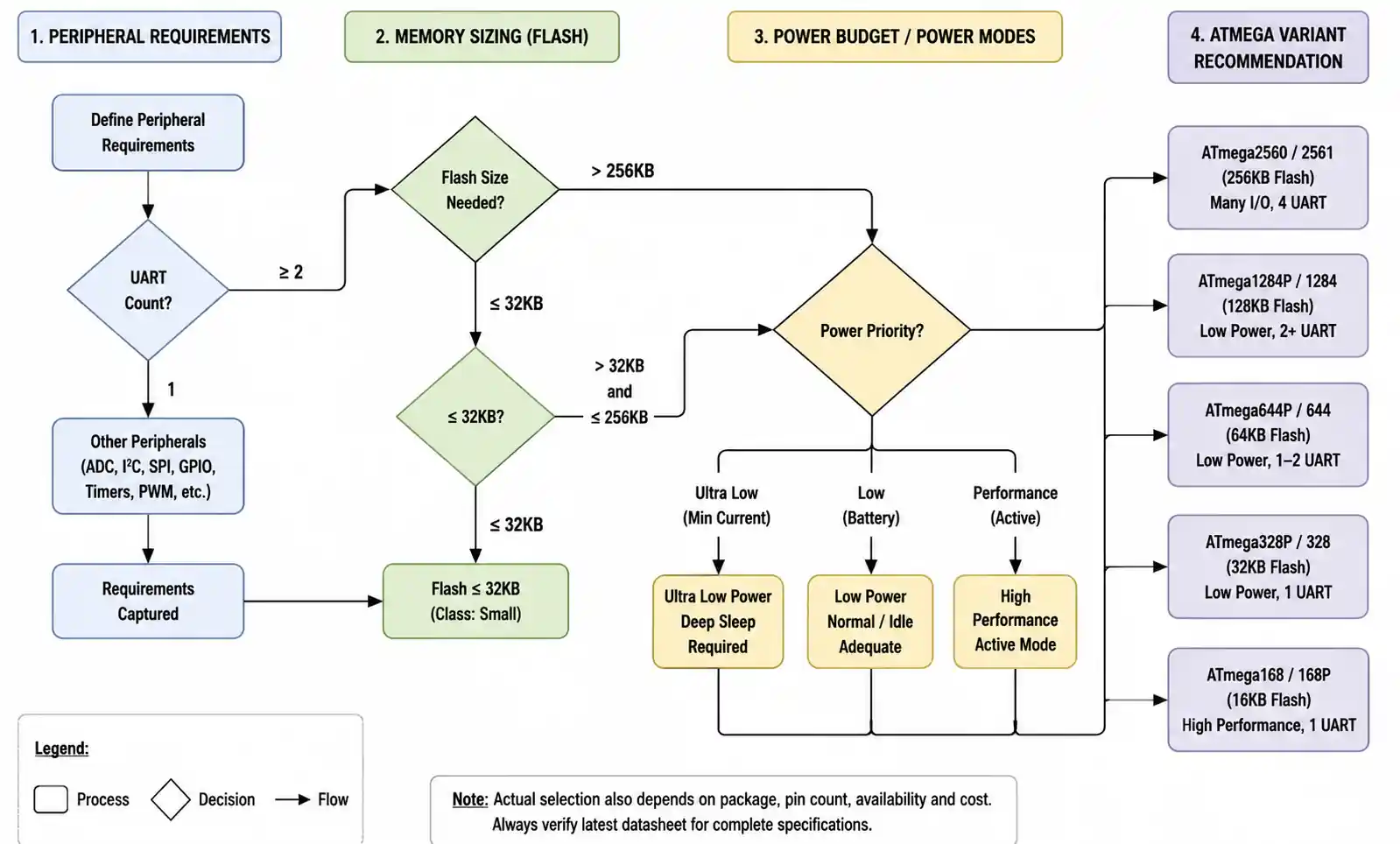
Step 1: Define Your Peripheral Requirements
List every interface your design needs: number of UART, SPI, I2C channels; PWM outputs for motor control or LED dimming; external interrupt pins for button interfaces or sensor triggers. ATmega peripherals are fixed—you cannot add a second UART if your initial selection has only one. Pay attention to pin multiplexing: on smaller packages, you may need to choose between SPI and certain GPIO pins.
Step 2: Calculate Memory Requirements
Estimate flash needs by compiling your baseline firmware with all required libraries. Add 30-40% margin for future features and debugging code that may need to remain in field units. For SRAM, sum your global variables, largest buffer, and stack. Use static analysis tools to identify stack depth; for interrupt-driven designs, assume worst-case interrupt nesting.
Step 3: Evaluate Processing and Timing Constraints
Determine if your application has hard real-time requirements. ATmega microcontrollers handle most control loops at 1 kHz easily, but DSP operations or communication protocols with tight timing (e.g., WS2812 LED control) may require specific clock speeds. Calculate your worst-case interrupt service routine (ISR) execution time and verify it fits within your tick period.
Step 4: Assess Power Budget
For battery-powered applications, profile your duty cycle: percentage of time in active mode, sleep mode selection, and wake-up frequency. ATmega power-down mode with periodic wake-up via watchdog timer is effective for sensor nodes that sample every few seconds. However, if you need to wake on external events, choose pin-change interrupt capable pins carefully as not all GPIO support wake-up.
Step 5: Consider Package and Pin Count
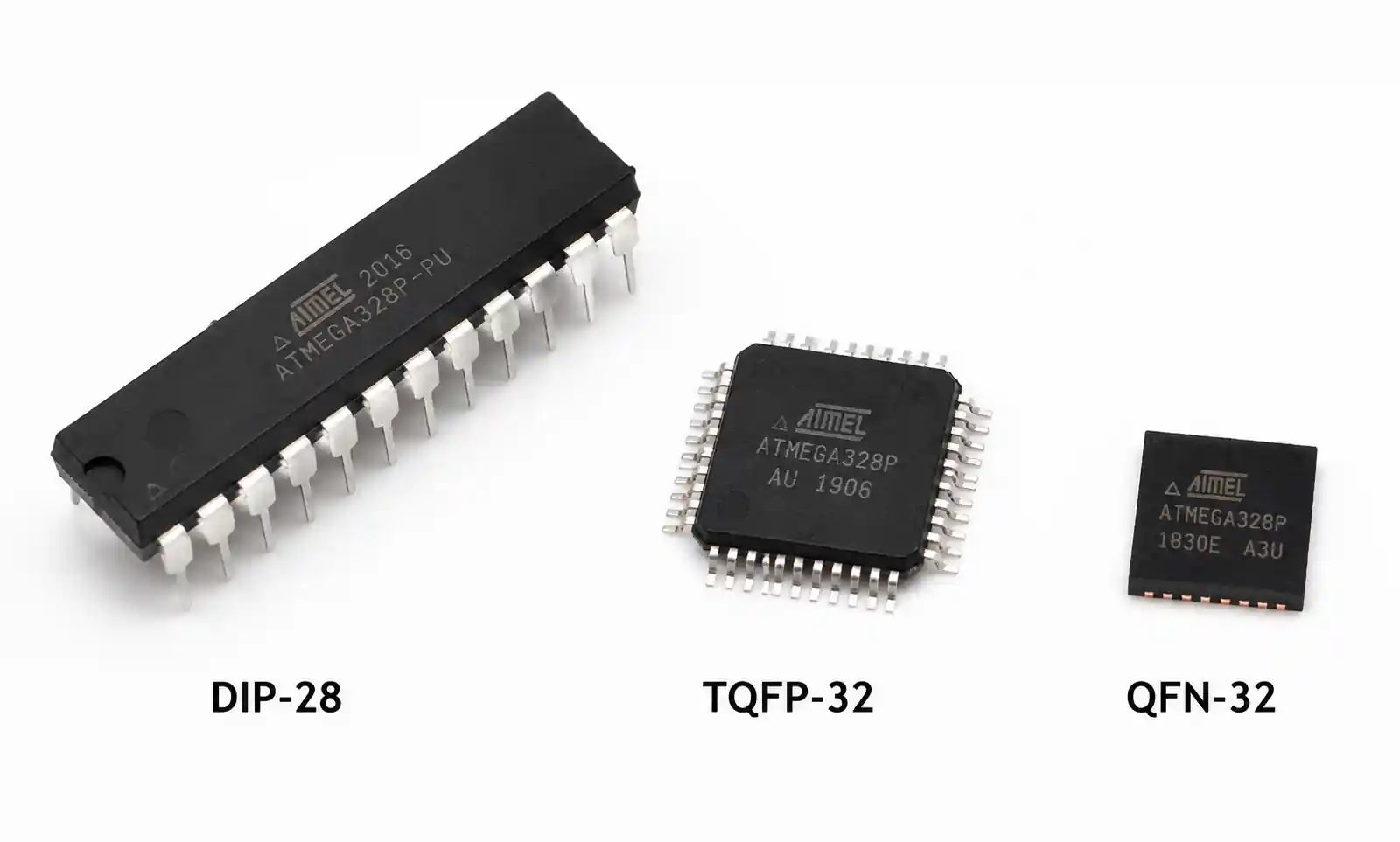
Smaller packages reduce PCB space and cost but limit available GPIO. Count every pin: power supplies, reset, crystal oscillator, programming interface (ISP requires 4 pins), and all application I/O. Don't forget that some pins have dual functions you cannot simultaneously use. DIP packages simplify prototyping but TQFP or QFN packages are standard for production.
Step 6: Verify Supply Chain and Lifecycle Status
Check component availability, lead times, and minimum order quantities with major distributors. Some older ATmega variants have longer lead times or higher pricing than newer family members with equivalent or better specifications. Microchip maintains good product longevity, but verify your chosen part isn't marked for obsolescence or in last-time-buy status.
4. Performance Comparison: ATmega328P vs ATmega2560 vs ATmega4809
Comparing three widely-used ATmega family members illustrates how specifications translate to application suitability. This comparison focuses on parameters that most significantly impact design decisions rather than exhaustive specification listing.
| Parameter | ATmega328P | ATmega2560 | ATmega4809 |
|---|---|---|---|
| Flash Memory | 32 KB | 256 KB | 48 KB |
| SRAM | 2 KB | 8 KB | 6 KB |
| EEPROM | 1 KB | 4 KB | 256 bytes |
| Max Clock Speed | 20 MHz | 16 MHz | 20 MHz |
| ADC Channels | 8 (10-bit) | 16 (10-bit) | 16 (10-bit) |
| UART Channels | 1 | 4 | 3 |
| Timers | 2x 8-bit, 1x 16-bit | 2x 8-bit, 4x 16-bit | 4x 16-bit |
| PWM Channels | 6 | 15 | 6 |
| GPIO Pins | 23 | 86 | 41 |
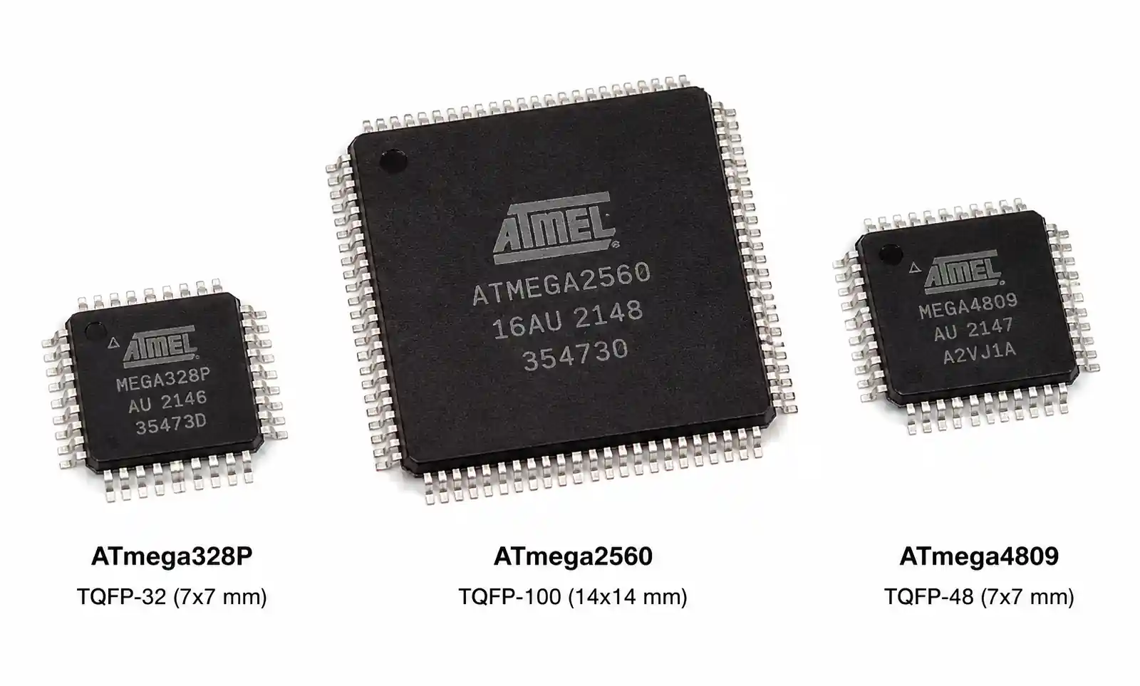
| Package Options | DIP-28, TQFP-32, QFN-32 | TQFP-100 | TQFP-48, QFN-48 |
| Operating Voltage | 1.8V - 5.5V | 1.8V - 5.5V | 1.8V - 5.5V |
| Active Current (@ 1 MHz, 3V) | 0.3 mA | 0.5 mA | 0.25 mA |
| Power-Down Current | 0.1 µA | 0.1 µA | 0.1 µA |
| Price (1ku, indicative) | $1.50 - $2.00 | $5.00 - $7.00 | $1.80 - $2.50 |
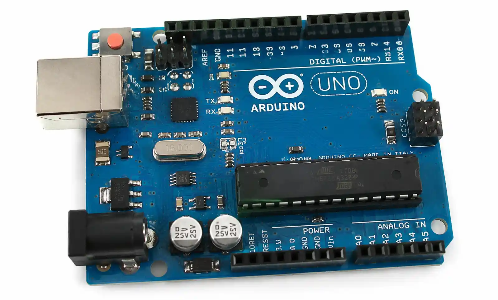
ATmega328P remains the go-to choice for cost-sensitive, moderate complexity applications. Its balance of 32KB flash and 2KB SRAM handles typical control algorithms, simple communication protocols, and moderate user interfaces. The single UART limits multi-device communication but can be supplemented with software serial for low-speed links. Most common in Arduino Uno platforms, its extensive community support and reference designs accelerate development.
ATmega2560 targets complex applications requiring multiple serial interfaces, extensive I/O control, or large lookup tables. The 256KB flash accommodates feature-rich firmware with multiple communication stacks. Four hardware UARTs enable simultaneous connections to GPS modules, cellular modems, debugging ports, and sensor networks without software multiplexing. The pin count makes routing more complex but eliminates external I/O expanders. Best suited for data loggers, multi-axis motion controllers, and gateway devices.
ATmega4809 represents the newer megaAVR 0-series with improved peripherals and lower power consumption. Its 6KB SRAM provides more buffer space than the 328P despite moderate flash size. Three UARTs and enhanced timers suit IoT edge devices that communicate with multiple sensors while maintaining low sleep current. The CCL (Configurable Custom Logic) peripheral implements simple glue logic in hardware, reducing CPU intervention. Consider this for battery-powered industrial sensors and building automation nodes.
The critical selection factor is UART count for multi-interface designs and flash size for feature-rich applications. For projects growing beyond ATmega328P capabilities, the 4809 offers better value than jumping directly to the 2560 unless you specifically need 80+ GPIO pins or 256KB program space.
5. Design Considerations and Common Pitfalls
Successful ATmega designs require attention to details that datasheets mention briefly but field experience proves critical. These considerations prevent common failures seen in production.
Decoupling and Power Supply Design
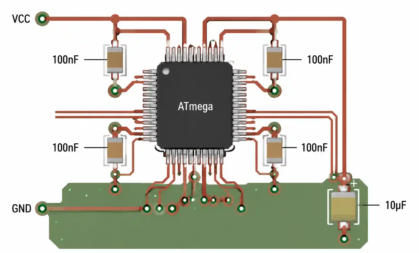
Place a 100 nF ceramic capacitor (X7R or X5R dielectric) within 5 mm of each VCC pin, connected to the nearest ground pin with minimal trace length. ATmega devices have multiple VCC/GND pairs; decouple all of them individually. A common mistake is sharing decoupling capacitors between multiple power pins through longer PCB traces, which increases supply impedance at high frequencies. Add one 10 µF tantalum or ceramic capacitor near the MCU for bulk energy storage during load transients. For analog-heavy applications, use a ferrite bead between AVCC and VCC to isolate ADC supply noise, with separate decoupling on AVCC.
Crystal Oscillator Selection and Layout
External crystals provide better frequency accuracy than internal RC oscillators (±1% vs ±10% tolerance). Position the crystal and its load capacitors within 10 mm of the XTAL1/XTAL2 pins. Keep crystal traces short, direct, and away from high-speed digital signals or switching power supply traces. Never route signals under the crystal—this area should be a ground plane. Load capacitor values depend on crystal specification and PCB parasitic capacitance; typical values are 18-22 pF for 16 MHz crystals. Verify your crystal's drive level specification matches the ATmega's output; exceeding crystal drive level causes frequency drift and premature crystal failure.
Reset Circuit and Programming Interface
Include a 10 kΩ pull-up resistor on the RESET pin to prevent spurious resets from EMI. If using external reset buttons, add a 100 nF capacitor to ground to debounce mechanical switch contacts. For In-System Programming (ISP), route the MISO, MOSI, SCK, RESET, VCC, and GND signals to a 6-pin header. Place this header in an accessible location; forgetting to include ISP access requires field units to be returned for firmware updates. Ensure ISP signal traces are not excessively long (keep under 150 mm) to prevent programming reliability issues at higher SCK frequencies.
ADC Input Protection and Filtering
The ATmega ADC input pins are vulnerable to voltages exceeding VCC + 0.5V or below GND - 0.5V. Use series resistors (1-10 kΩ) combined with clamping diodes (Schottky BAT54 series) to protect inputs from overvoltage transients. For noisy environments, add an RC filter before the ADC pin: a 1 kΩ resistor followed by a 100 nF capacitor creates a low-pass filter that attenuates high-frequency noise. Remember this filter introduces a time constant that affects conversion speed; reduce capacitance if sampling rate is critical.
I/O Pin Current Limits
Each ATmega GPIO pin sources or sinks a maximum of 40 mA absolute maximum rating, but the recommended continuous current is 20 mA. More critically, the total current through all VCC and GND pins combined must not exceed 200 mA. Driving multiple LEDs or relay coils directly from GPIO pins often violates this limit. Use external drivers (transistors, MOSFETs, or dedicated driver ICs) for loads exceeding 10 mA per pin or when driving more than four pins simultaneously at high current.
Brownout Detection Configuration
Enable brownout detection (BOD) via fuse settings to prevent firmware corruption when supply voltage drops below safe operating levels. The ATmega enters reset when VCC falls below the BOD threshold, preventing erratic execution or memory corruption. For battery-powered designs, balance BOD level against usable battery capacity: setting BOD too high wastes battery energy, too low risks brownout-induced failures. Typical settings are 4.3V for 5V systems, 2.7V for 3.3V systems.
Fuse Bit Programming Errors
ATmega fuses configure critical operating parameters: clock source, clock division, BOD level, and programming lock bits. Incorrect fuse settings are the most common cause of "bricked" ATmegas. Never disable the SPIEN fuse—this permanently prevents ISP programming, requiring high-voltage parallel programming to recover. When changing clock fuse settings, ensure your programmer can supply the new clock frequency or provide an external clock during initial programming. Document your fuse settings in version control; losing fuse configuration information complicates production programming.
6. Supply Chain and Sourcing Considerations
Component availability and sourcing strategy significantly impact project timelines and manufacturing costs. The ATmega family's market position offers advantages, but engineers must navigate lead time variability and part lifecycle status.
Authorized Distributor Landscape
Source ATmega microcontrollers from authorized Microchip distributors including Digi-Key, Mouser, Arrow, Avnet, and Newark. Authorized channels guarantee genuine parts with full warranty and traceability. Pricing typically ranges from $1.50 to $7.00 depending on variant, with volume discounts starting at 100 units (5-10% reduction) and significant breaks at 1,000+ units (15-25% reduction). For production volumes exceeding 10,000 units annually, direct Microchip engagement or franchise distributor agreements offer additional cost optimization.
Lead Time Management
Standard lead times for popular ATmega variants (328P, 2560, 4809) range from in-stock to 8-12 weeks depending on global demand. During semiconductor shortages, lead times extend to 26-52 weeks. Implement a dual-sourcing strategy by qualifying alternative ATmega family members that meet your specifications. For example, if ATmega328P faces long lead times, evaluate ATmega328PB (enhanced variant with additional peripherals) or ATmega4809 as potential alternatives, recognizing that firmware modifications may be required.
Counterfeit Risk Mitigation
ATmega microcontrollers are occasionally counterfeited, particularly the popular 328P variant. Red flags include pricing significantly below market rates (>30% discount), sellers without authorized distributor credentials, and chips with inconsistent package markings. Counterfeit ATmegas may be remarked lower-grade parts, salvaged components, or non-functional reproductions. For critical applications, implement incoming inspection testing: verify device signature via ISP, test peripheral functionality, and perform temperature stress testing on sample units.
Obsolescence and Product Lifecycle
Microchip maintains excellent product longevity; many ATmega variants introduced in the early 2000s remain in active production. However, some older package options (PDIP for certain variants) face limited availability. Check Microchip's PCN (Product Change Notification) system for lifecycle announcements. For new designs with 10+ year production horizons, prefer newer megaAVR 0-series and 1-series families (like ATmega4809) which have stronger long-term support commitments.
Alternative Component Strategy
Maintain a bill-of-materials (BOM) that identifies acceptable alternatives for your primary ATmega selection. Document the firmware modifications required for each alternative. This strategy reduces project risk when specific part numbers face allocation or end-of-life scenarios. Within the ATmega family, pin-compatible alternatives exist (e.g., ATmega48/88/168/328 share pinouts with different memory sizes), simplifying substitution.
The following table outlines typical sourcing parameters for popular ATmega variants:
| Parameter | ATmega328P | ATmega2560 | ATmega4809 |
|---|---|---|---|
| Typical Lead Time (Stock) | In-stock to 12 weeks | In-stock to 16 weeks | In-stock to 10 weeks |
| MOQ (Distributor) | 1 unit | 1 unit | 1 unit |
| MOQ (Factory Direct) | 2,000 units | 500 units | 2,000 units |
| Common Package Stock | TQFP-32, DIP-28 | TQFP-100 | TQFP-48 |
| Alternative Variants | 328PB, 168, 88 | None direct | 3209, 1609 |
| AEC-Q100 Available | Limited | No | Yes (select SKUs) |
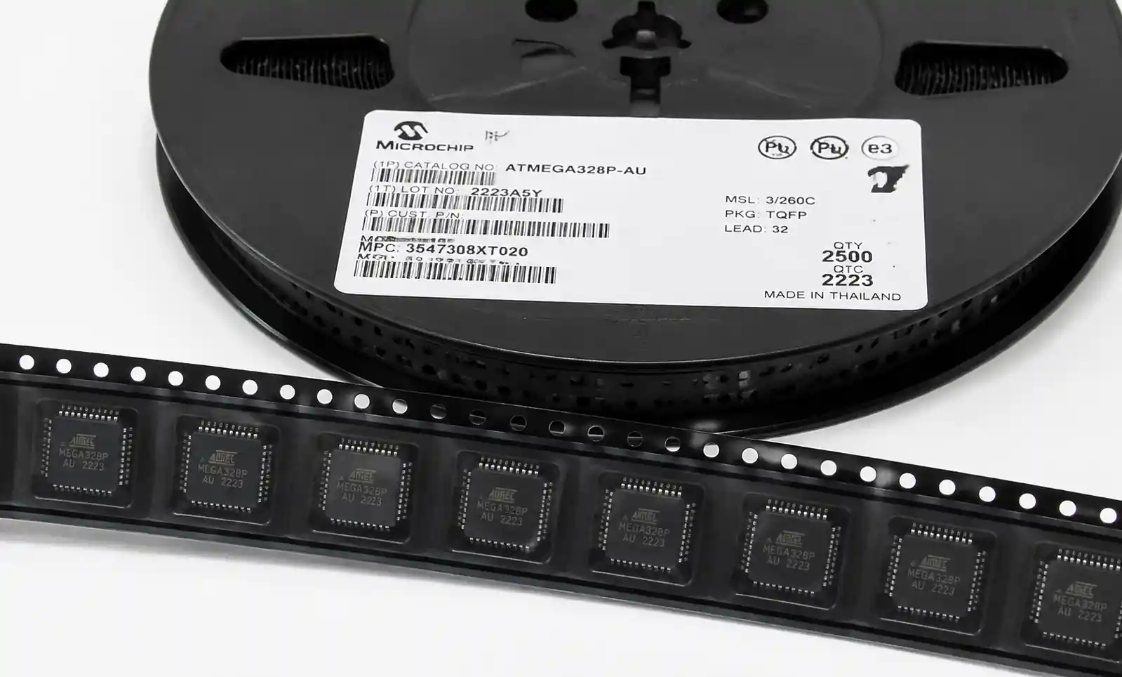
For applications requiring automotive qualification, verify specific part numbers with "automotive" suffix (e.g., ATmega328P-AU) as standard commercial variants do not meet AEC-Q100 standards.
7. FAQ
Q: What is the main difference between ATmega and ATtiny microcontrollers?
ATmega microcontrollers target applications requiring more memory, peripherals, and I/O pins compared to ATtiny devices. ATmega variants start at 2KB flash and scale to 256KB, while ATtiny typically ranges from 512 bytes to 8KB. ATmega devices include more sophisticated peripherals like multiple UARTs, larger ADC channel counts, and additional timers. Choose ATtiny for space-constrained, cost-sensitive applications with simple control tasks; select ATmega when you need communication interfaces, larger programs, or more I/O flexibility.
Q: Can I use the Arduino IDE for commercial ATmega-based products?
Yes, the Arduino IDE and libraries are open-source and suitable for commercial use under their respective licenses (LGPL for core libraries). However, for production firmware, consider transitioning to Microchip Studio (formerly Atmel Studio) or AVR-GCC toolchain directly for better optimization, debugging capabilities, and professional development practices. Arduino libraries simplify prototyping but often include overhead unsuitable for resource-constrained production code. Verify code size and performance meet your requirements before committing to Arduino-based firmware architecture.
Q: How do I calculate the required decoupling capacitor value for my ATmega design?
Use a 100 nF (0.1 µF) X7R ceramic capacitor on each VCC pin, placed as close as possible to the pin with short, wide traces to ground. Add one 10 µF tantalum or ceramic capacitor near the MCU for bulk storage. This combination handles high-frequency switching noise (100 nF) and larger current transients (10 µF). For ADC-intensive applications, add an additional 100 nF capacitor on AVCC with a ferrite bead isolating AVCC from VCC. These values are standard across most ATmega applications; adjust only if you have verified power integrity issues via oscilloscope measurement.
Q: What are the most common failure modes for ATmega microcontrollers and how can I prevent them?
The three most common failures are: 1) ESD damage to I/O pins—prevent with series resistors (1 kΩ) and clamping diodes on external-facing connections; 2) Incorrect fuse settings bricking the device—always document fuse configurations and avoid disabling SPIEN; 3) Latchup from input voltages exceeding VCC or below GND—add input protection circuits on all external signals. Additionally, brownout detection prevents firmware corruption during power supply instability. Proper PCB layout with adequate decoupling prevents intermittent resets and erratic behavior caused by supply noise.
Q: Is there a pin-compatible upgrade path if my project outgrows the ATmega328P?
Within the ATmega48/88/168/328 family, devices are pin-compatible with only memory size differences, enabling direct upgrades. However, for more substantial capability increases, no direct pin-compatible path exists to ATmega2560 or newer megaAVR families. For future scalability, design your firmware with hardware abstraction layers that simplify porting to different MCUs. Alternatively, select a more capable variant initially with sufficient headroom for feature growth. Overprovisioning by 50% in flash and SRAM costs $0.50-1.00 more but avoids expensive redesigns.
Q: How do I handle long lead times for ATmega microcontrollers in my production schedule?
Implement these strategies: 1) Place non-cancellable, non-returnable (NCNR) orders 6-12 months ahead for production volumes based on forecast; 2) Qualify alternative ATmega family members with similar specifications to create sourcing flexibility; 3) Maintain 3-6 months of safety stock for critical products; 4) Engage with distributors for inventory management programs where they hold consignment stock. For prototype and low-volume production, utilize distributor stock; for volumes exceeding 5,000 units annually, establish direct Microchip factory allocations.
Q: What programming interface should I use for production ATmega programming?
For production, use In-System Programming (ISP) via the SPI interface, which requires six connections: MISO, MOSI, SCK, RESET, VCC, and GND. ISP programmers range from low-cost USBasp devices ($10-20) for prototyping to automated gang programmers ($500-2000+) for high-volume manufacturing. Include a 6-pin ISP header on your PCB even if you plan to pre-program chips; this enables field updates and failure analysis. For security-sensitive applications, program lock bits after loading firmware to prevent code readout, but note this also prevents ISP-based updates—plan your security strategy accordingly.
Q: Can ATmega microcontrollers operate reliably in automotive or industrial temperature ranges?
Standard ATmega variants are rated for industrial temperature range (-40°C to +85°C). For automotive applications, select parts with automotive-grade suffixes that meet AEC-Q100 qualification and extend to +105°C or +125°C. The ATmega328P-AU and certain ATmega4809 variants offer automotive qualification. Extended temperature operation affects maximum clock frequency and requires derating analysis—consult the datasheet's temperature vs. frequency specifications. For extreme environments, add thermal management and select components with appropriate temperature coefficients for all passive components.
8. Conclusion and Recommended Next Steps
ATmega microcontrollers deliver reliable, cost-effective solutions for embedded applications where 8-bit processing, extensive peripheral integration, and mature development ecosystems provide clear advantages over more complex 32-bit alternatives. Your selection should prioritize peripheral requirements first, followed by memory sizing with adequate headroom, and power budget alignment with your application's duty cycle.
For typical control applications with moderate I/O and single communication interfaces, the ATmega328P offers the best balance of capability, cost, and community support. When your design requires multiple UARTs, extensive GPIO, or programs exceeding 32KB, the ATmega2560 justifies its higher cost through integrated functionality that eliminates external components. For modern IoT and battery-powered applications, evaluate the ATmega4809 and newer megaAVR 0-series for improved power efficiency and enhanced peripherals.
Before finalizing your selection, download the complete datasheet for your target ATmega variant and verify electrical specifications against your requirements. Pay particular attention to ADC characteristics if sensor interfacing is critical, and validate timer peripheral capabilities for PWM or timing-sensitive protocols. Use Microchip's parametric search tools to compare variants and identify the optimal balance for your application.
If you need application-specific guidance, reference designs are available through Microchip's website covering motor control, sensor interfaces, wireless connectivity, and power management. For production designs, engage with Microchip FAE (Field Application Engineer) teams or authorized distributors' technical support to validate your selection and review critical design elements.
Begin your development with evaluation boards (Arduino Uno for ATmega328P, Arduino Mega for ATmega2560) to prototype firmware and verify peripheral functionality before committing to custom hardware. This approach reduces risk and accelerates time-to-market by validating assumptions early in the design cycle.