


DC/DC Converter vs LDO Regulator: Complete Selection Guide for Power Supply Design
When designing power supply circuits, choosing between a DC/DC converter and an LDO (Low Dropout) regulator is one of the most critical decisions that impacts efficiency, thermal performance, cost, and board space. This guide provides a parameter-by-parameter comparison and practical selection methodology to help engineers and procurement teams make informed decisions based on application requirements.
Table of Contents
- Introduction: Why This Choice Matters
- Key Technical Parameters Explained
- Parameter-by-Parameter Comparison
- Application Scenario Analysis
- Design Considerations and Common Pitfalls
- Cost, Board Space, and Supply Chain Comparison
- When to Use Which Option
- FAQ
- Conclusion
1. Introduction: Why This Choice Matters
Voltage regulation is fundamental to every electronic system, yet the choice between switching DC/DC converters and linear LDO regulators often gets oversimplified. In practice, this decision involves complex trade-offs between efficiency, noise performance, thermal management, component count, and total solution cost.
DC/DC converters use switching technology to achieve high efficiency across wide input voltage ranges, making them ideal for battery-powered devices and applications where thermal dissipation is a concern. LDO regulators offer superior noise performance and simpler implementation but convert excess voltage into heat, which limits their practical use to low dropout scenarios.
This guide is structured to help PCB design engineers, R&D teams, and procurement managers understand when each topology delivers optimal performance. We'll cover the technical fundamentals, provide comparison tables with real-world parameters, analyze common application scenarios, and address frequent design mistakes observed in production environments.
2. Key Technical Parameters Explained
Before comparing these two regulator types, it's essential to understand the key specifications that drive design decisions.
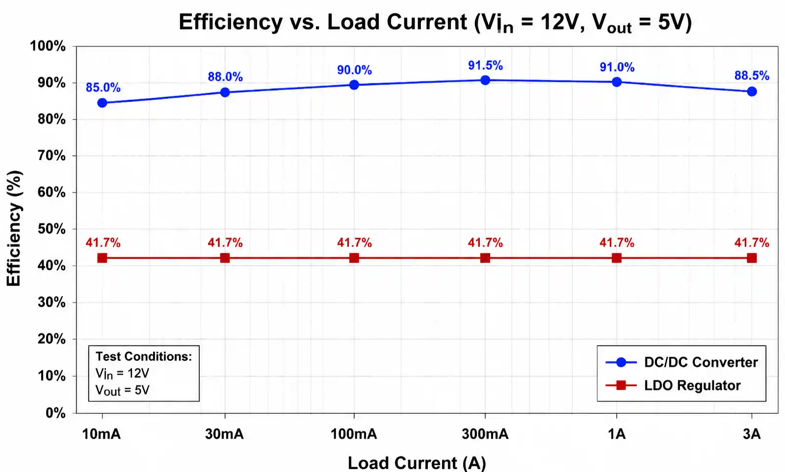
Efficiency is calculated as (Output Power / Input Power) × 100%. For DC/DC converters, efficiency typically ranges from 85% to 95% depending on switching frequency, load current, and input-output voltage differential. LDO efficiency equals (V_out / V_in) × 100%, meaning a 5V to 3.3V LDO operates at only 66% efficiency regardless of load current.
Dropout Voltage defines the minimum input-output voltage differential required for regulation. Modern LDOs achieve dropout voltages as low as 100-300mV at full load, while DC/DC converters don't have a traditional dropout specification but require minimum input voltage to maintain switching operation.
Output Voltage Ripple measures AC noise on the regulated output. LDOs typically produce 10-50µV RMS ripple, while switching regulators generate 10-50mV ripple at the switching frequency, requiring careful output filtering for noise-sensitive loads.
Load Transient Response indicates how quickly the regulator responds to sudden load current changes. This parameter is critical for digital loads with pulsed current consumption. LDOs typically respond within microseconds due to their simple feedback loop, while DC/DC converters may take longer depending on control bandwidth and output capacitance.
Quiescent Current (I_q) represents the regulator's own power consumption independent of load current. Low-quiescent-current LDOs achieve 1-50µA, making them suitable for battery backup circuits. DC/DC converters typically consume 10-100µA in continuous mode, though some ultralow-power designs achieve sub-1µA in pulse-skipping mode.
Power Supply Rejection Ratio (PSRR) measures the regulator's ability to attenuate input voltage noise. LDOs excel here with 40-80dB PSRR at low frequencies, degrading at higher frequencies. DC/DC converters provide poor PSRR at the switching frequency but can be improved with post-filtering.
3. Parameter-by-Parameter Comparison
The following table compares key technical specifications between typical switching DC/DC converters and LDO linear regulators. These values represent mainstream components; specialized devices may exceed these ranges.
| Parameter | DC/DC Converter | LDO Regulator | Impact on Design |
|---|---|---|---|
| Efficiency | 85-95% (typical) | (V_out/V_in) × 100% | DC/DC reduces thermal dissipation and extends battery life |
| Dropout Voltage | Not applicable (min V_in required) | 100-300mV at full load | LDO works with minimal headroom voltage |
| Output Ripple | 10-50mV (at f_sw) | 10-50µV RMS | LDO superior for noise-sensitive analog circuits |
| Quiescent Current | 10-100µA (continuous mode) | 1-50µA (modern designs) | LDO advantage in ultra-low-power standby |
| PSRR @ 1kHz | 20-40dB | 60-80dB | LDO significantly better at rejecting input noise |
| Load Transient | Limited by control loop BW | Fast (µs range) | LDO responds faster to sudden load changes |
| EMI Generation | High (requires PCB layout care) | Minimal (no switching) | LDO simpler from EMC perspective |
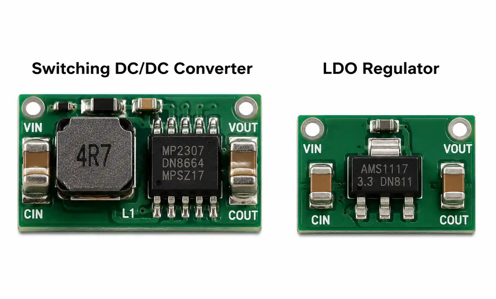
| External Components | 5-10 (inductor, caps, diodes) | 2-3 (input/output caps only) | LDO reduces BOM and board area |
| Component Height | Inductor adds 2-4mm | Flat (IC only) | LDO advantage in thickness-constrained designs |
| Solution Cost | Higher (inductor, IC complexity) | Lower (simple IC) | LDO more economical for low-current applications |
This comparison reveals that neither topology is universally superior. The optimal choice depends on the specific requirements of input voltage range, output current, efficiency targets, noise tolerance, and physical constraints. In high-efficiency applications with significant input-output voltage differential, DC/DC converters recover their higher component cost through reduced thermal management requirements and smaller heatsinks.
For low-dropout applications below 500mA where output noise must remain under 100µV, LDOs provide a simpler, lower-cost solution despite their efficiency disadvantage. Many designs employ both topologies: a switching pre-regulator for efficient voltage conversion followed by an LDO post-regulator for noise filtering.
4. Application Scenario Analysis
Different applications prioritize different parameters, making the regulator choice highly context-dependent. This section analyzes five common scenarios and recommends the appropriate topology based on dominant design constraints.
| Application Type | Input Voltage | Output Current | Priority Parameters | Recommended Topology | Reasoning |
|---|---|---|---|---|---|
| Battery-powered IoT sensor | 2.7-4.2V (Li-ion) | 10-50mA average | Efficiency, I_q, sleep current | DC/DC with pulse-skip mode | Efficiency extends battery life; pulse-skip reduces I_q in sleep |
| Automotive infotainment | 6-18V (12V nominal) | 2-5A | Input transient tolerance, wide V_in range | Switching buck converter | Large V_in-V_out differential; LDO thermal dissipation impractical |
| RF power amplifier supply | 3.6-5V | 500mA-2A | Low noise, fast transient response | LDO (possibly with pre-regulator) | PSRR and low ripple critical for RF performance |
| Industrial sensor interface | 24V industrial bus | 50-200mA | Wide input range, isolation | Isolated DC/DC converter | High input voltage and isolation requirement |
| USB-powered portable device | 5V (USB) | 100-500mA | Cost, board space, EMI | LDO (3.3V output) | Low dropout, simple design, no switching noise |
| High-current digital core | 5V or 12V rail | 5-20A | Efficiency, transient response | Multiphase buck converter | High current demands high efficiency; LDO would dissipate excessive heat |
Battery-Powered Applications: When operating from a single-cell lithium battery (2.7-4.2V range), the choice depends on output voltage and current. For 1.8V or 3.3V outputs at moderate current (>100mA), a switching buck converter provides 85-90% efficiency compared to an LDO's 43-79% efficiency across the battery discharge curve. However, for ultra-low-power modes below 10µA, modern LDOs with sub-1µA quiescent current may provide better total efficiency than a DC/DC converter with higher quiescent current.
Automotive Applications: The wide input voltage range (6-18V for 12V systems, 18-40V for 24V systems) combined with load dump transients up to 40V makes switching regulators mandatory for significant current loads. An LDO attempting to regulate from 14V to 5V at 1A would dissipate 9W continuously, requiring substantial heatsinking. Automotive-qualified buck converters with integrated high-side switches simplify this design while maintaining high efficiency across the input voltage range.
Noise-Sensitive Analog Applications: RF circuits, precision ADCs, and low-noise amplifiers demand supply ripple below 100µV and excellent PSRR. Here, LDOs remain the preferred solution. When efficiency is also a concern, a hybrid approach works well: use a switching pre-regulator to drop the voltage efficiently (e.g., 12V to 5V), then use an LDO for the final regulation (5V to 3.3V) where the efficiency penalty is minimal but noise rejection is maximized.
5. Design Considerations and Common Pitfalls
Based on field experience and design reviews, several recurring mistakes occur when implementing voltage regulators. Understanding these pitfalls helps avoid costly board respins.
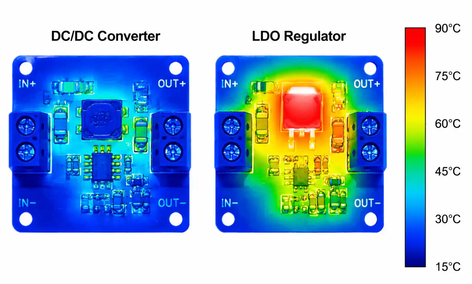
Thermal Management Miscalculations: The most common LDO mistake is underestimating thermal dissipation. Power dissipation equals (V_in - V_out) × I_load. A 12V to 5V LDO supplying 500mA dissipates 3.5W continuously. With a typical θ_JA of 40-60°C/W for SOT-223 packages without heatsinking, junction temperature rises 140-210°C above ambient. This exceeds the maximum junction temperature of most ICs (125-150°C), causing thermal shutdown or shortened lifetime. Always calculate worst-case thermal dissipation and verify that T_j remains within limits: T_j = T_ambient + (Power × θ_JA).
DC/DC Layout Errors: Switching regulators are sensitive to PCB layout due to high di/dt switching currents. The most critical error is excessive loop area in the input capacitor-switch-diode-output capacitor path. This loop acts as an antenna radiating EMI and creates ground bounce. Best practice requires placing input capacitors within 5mm of the V_in pin, minimizing trace length between the switching node and catch diode, and using a solid ground plane. The feedback divider should route away from the switching node to avoid coupling high-frequency noise into the control loop.
Output Capacitor Selection: Both regulator types require careful output capacitor selection, but for different reasons. LDOs need sufficient capacitance (typically 10-22µF ceramic) to maintain stability; some LDOs specify maximum ESR requirements while others specify minimum ESR for stability. Always consult the datasheet stability curves. DC/DC converters need output capacitance to provide energy storage during switching cycles and control output ripple. The ripple voltage equals ΔI_L / (8 × f_sw × C_out), where ΔI_L is the inductor ripple current. Using the wrong capacitor type (high-ESR aluminum instead of low-ESR ceramic) can increase ripple beyond acceptable limits.
Dropout Voltage Violations: A common mistake occurs when designing with marginal headroom voltage. If the input voltage can drop to 3.5V and you need 3.3V output, the available dropout is only 200mV. While the LDO datasheet may specify 150mV typical dropout, this value varies with load current and temperature. At maximum load and high temperature, dropout can increase to 300mV, causing the output to fall out of regulation. Always design with at least 20-30% margin above the specified dropout voltage at maximum load current.
Load Transient Response: Digital loads with pulsed current consumption (microcontrollers entering/exiting sleep mode, RF PA transmit bursts) create sudden load steps. If the regulator cannot respond quickly enough, output voltage sags or overshoots beyond the acceptable tolerance band. For LDOs, ensure adequate output capacitance (fast ceramic capacitors, not slow aluminum electrolytics) to supply charge during transients. For DC/DC converters, the control loop bandwidth limits transient response; some applications require additional feedforward capacitance or may benefit from hysteretic control modes with faster response than fixed-frequency PWM.
Input Voltage Ripple Coupling: When cascading multiple regulators or operating from a noisy input bus, ensure adequate input filtering. An LDO's PSRR degrades with frequency (typically 20-30dB at 100kHz), so high-frequency noise on V_in appears on V_out with only moderate attenuation. Adding a small LC filter on the LDO input improves PSRR at frequencies beyond the LDO's internal bandwidth. For DC/DC converters, input ripple at the switching frequency can couple through parasitic capacitance, requiring careful board layout and adequate input capacitance.
6. Cost, Board Space, and Supply Chain Comparison
Beyond technical performance, practical considerations of cost, physical size, and component availability influence the final design choice.
| Factor | DC/DC Converter | LDO Regulator | Practical Impact |
|---|---|---|---|
| IC Unit Cost | $0.50-$3.00 (depends on I_out, integration) | $0.20-$1.00 (depends on I_out, features) | LDO has lower IC cost for low-current applications |
| External Components | Inductor ($0.30-$2.00), caps, diodes | Input/output caps only ($0.10-$0.30 total) | DC/DC adds $0.50-$2.50 in passives |
| Total BOM Cost | Higher for <500mA, competitive at higher currents | Lower for <500mA applications | Crossover point around 500mA-1A |
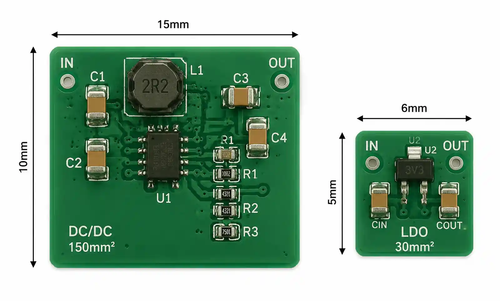
| PCB Area | 100-300mm² (includes inductor keepout) | 20-50mm² (IC + small caps) | LDO advantage in space-constrained designs |
| Component Height | 2-4mm (inductor height) | <1mm (flat ceramic caps) | LDO critical for thin industrial designs |
| Assembly Complexity | Higher (inductor orientation, layout-sensitive) | Lower (standard SMT process) | LDO reduces manufacturing risks |
| Lead Time Risk | Inductor availability varies | Standard capacitors readily available | Power inductors occasionally face allocation |
| Design Time | 2-5 days (simulation, layout optimization) | 0.5-1 day (straightforward design) | LDO faster time-to-market |
Cost Analysis: For low-current applications (below 500mA), LDOs typically provide a lower-cost solution when all factors are considered. A basic 500mA LDO in SOT-23 package costs $0.20-$0.40, requires only two ceramic capacitors ($0.10 total), and occupies minimal board space. An equivalent DC/DC converter requires a $0.50-$1.00 IC, a $0.40-$0.80 inductor, input/output capacitors, and possibly a catch diode, totaling $1.50-$2.50. However, at higher currents (above 2A), the efficiency advantage of DC/DC converters reduces heatsink costs and may enable smaller power supply components, shifting the economic balance.
Board Space Considerations: Physical size constraints often dictate the choice. The inductor in a DC/DC converter occupies 20-50mm² of PCB area (for 1-3A designs) and requires additional keepout area around it to minimize EMI coupling. In contrast, an LDO solution occupies 20-30mm² total including decoupling capacitors. For wearable devices, thin IoT sensors, or densely populated boards, the LDO's smaller footprint provides a decisive advantage despite its efficiency disadvantage.
Supply Chain Factors: During component shortages, power inductors with specific inductance, saturation current, and DCR ratings can face long lead times (12-26 weeks) or allocation. Standard LDOs and ceramic capacitors typically have broader second-source options and shorter lead times. When designing for manufacturing at scale, consider the supply chain robustness of each approach. Using a common LDO family across multiple products reduces inventory complexity, while DC/DC designs may require unique inductors for each voltage/current combination.
7. When to Use Which Option
After analyzing technical parameters, application requirements, and practical constraints, we can establish clear decision criteria for selecting between DC/DC converters and LDO regulators.
Use an LDO regulator when:
- Input-output voltage differential is less than 1.5V and output current is below 500mA. The efficiency penalty remains manageable, and thermal dissipation stays within reasonable limits for standard packages.
- Output noise must remain below 100µV RMS, such as powering precision analog-to-digital converters, voltage references, or RF local oscillators. The LDO's superior PSRR and inherently low output noise cannot be matched by switching regulators without extensive post-filtering.
- Board space is severely constrained, particularly in thickness-limited applications. The absence of an inductor allows LDO solutions to fit in sub-1mm height profiles.
- Design time is critical, and you need a proven, low-risk solution. LDOs require minimal external components and are less sensitive to layout variations.
- The load is a noise-sensitive analog circuit located on the same board, where conducted and radiated EMI from a switching regulator would require extensive shielding and filtering.
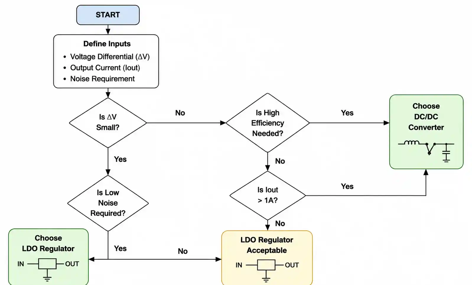
Use a DC/DC converter when:
- Input-output voltage differential exceeds 3V, or output current exceeds 500mA. Above these thresholds, the thermal dissipation in an LDO becomes impractical, requiring large heatsinks that negate the size advantage.
- Efficiency is a primary design goal, particularly in battery-powered systems where extended runtime is critical. The 85-95% efficiency of DC/DC converters significantly outperforms LDOs when V_in differs substantially from V_out.
- Input voltage range is wide (greater than 2:1 ratio), such as automotive applications (9-18V) or industrial systems (18-36V). LDOs would dissipate excessive power at high input voltages.
- Output current exceeds 2A. At these current levels, the cost of an adequate heatsink for an LDO exceeds the additional component cost of a switching solution.
- Thermal management is constrained due to limited airflow, high ambient temperature, or enclosed packaging where convective cooling is inadequate.
Hybrid solutions combining both:
Many advanced designs use a two-stage approach: a switching pre-regulator provides efficient voltage conversion, followed by an LDO post-regulator for noise filtering. For example, in a mixed-signal system powered from 12V, use a buck converter to efficiently drop to 5V (92% efficiency, 7% loss), then use an LDO to generate 3.3V analog supply (66% efficiency, but only 34% loss of the small differential). This approach achieves approximately 61% total efficiency while delivering ultra-low-noise 3.3V power, compared to 27.5% efficiency for a direct 12V-to-3.3V LDO.
8. FAQ
Q: Can I parallel multiple LDOs to increase output current capability?
A: Paralleling LDOs is possible but not recommended. Slight differences in output voltage between devices cause current sharing imbalances, with one LDO carrying most of the load. Some manufacturers offer LDOs with current-sharing pins designed for parallel operation, but for currents above 3A, switching regulators provide a more reliable solution.
Q: Why does my DC/DC converter produce more noise than the datasheet specifies?
A: Measured output ripple is highly dependent on probing technique and PCB layout. Use proper measurement techniques: probe ground spring instead of long ground leads, measure at the load location rather than at the regulator output, and ensure adequate input/output bypassing. Poor layout with long trace inductance amplifies switching noise beyond the datasheet specification which assumes optimal layout.
Q: How do I calculate the required inductor value for a buck converter?
A: Inductor value determines ripple current. Use L = (V_out × (V_in - V_out)) / (ΔI_L × f_sw × V_in), where ΔI_L is the desired ripple current (typically 20-40% of maximum load current) and f_sw is the switching frequency. Ensure the inductor's saturation current exceeds peak inductor current and DCR is low enough to maintain efficiency.
Q: What causes an LDO to oscillate, and how can I fix it?
A: LDO oscillation typically results from inadequate or incorrect output capacitance. Most LDOs specify minimum capacitance and ESR range for stability. Using only high-capacitance, ultra-low-ESR ceramic capacitors can destabilize some LDO designs that require minimum ESR for compensation. Check the datasheet stability curves and ensure your output capacitor falls within the stable region. Adding a small series resistance (0.1-1Ω) sometimes stabilizes problematic configurations.
Q: Can I use a DC/DC converter to generate a negative output voltage?
A: Yes, using inverting buck-boost or Cuk topologies. Standard buck converters only step down voltage with positive outputs. For negative voltages, select an inverting topology or use a dedicated negative output regulator. LDOs require a negative input voltage to generate a negative output, so they work only if you already have a negative supply rail.
Q: How do I handle automotive load dump transients with a DC/DC converter?
A: Load dump transients in 12V automotive systems can reach 40V for 400ms. Use a DC/DC converter rated for the full transient range, or add input protection with a TVS diode and series resistor to clamp transients below the converter's maximum rating (typically 40-42V for automotive-grade buck converters). Always verify your design meets ISO 7637-2 pulse testing requirements.
Q: What are common failure modes for each regulator type?
A: LDOs typically fail from thermal overstress (exceeding maximum junction temperature), input/output overvoltage (exceeding absolute maximum ratings), or reverse voltage on the output. DC/DC converters fail from inductor saturation under overload, inadequate input bypassing causing voltage spikes that damage the IC, or avalanche breakdown in the switching MOSFET during turn-off if there's excessive ringing.
Q: Is there a significant difference in EMI between synchronous and non-synchronous DC/DC converters?
A: Synchronous converters replace the catch diode with a low-side MOSFET, improving efficiency but potentially increasing EMI due to faster switching edges and body diode reverse recovery in the low-side FET. Non-synchronous designs have slightly higher losses but may generate less high-frequency EMI. For EMI-critical applications, evaluate both topologies with conducted and radiated emissions testing rather than assuming one is universally better.
9. Conclusion
Picking between a DC‑DC converter and an LDO? There’s no universal answer—it depends on your specific needs. If the dropout is small (under 1.5 V) and current stays below 500 mA, an LDO is simpler, cheaper, and quieter. For larger voltage drops, higher currents, or tight efficiency requirements, a switching regulator wins despite its extra complexity, thanks to far better efficiency and thermal performance.
Many clever designs combine both: a DC‑DC for bulk power conversion, followed by an LDO to clean up noise for sensitive analog circuits. That gives you the best overall performance.Before you commit, do the math: calculate LDO power dissipation at max load and minimum input voltage, and lay out your DC‑DC carefully—follow the manufacturer's guidelines for critical current loops. Always leave some margin. For tricky applications, reach out to the FAE team or check reference designs.
And for production, qualify samples from at least two suppliers to secure your second-source options and reduce supply chain risk.