



Understanding Drift and Diffusion Currents in Semiconductors: A Complete Guide
Semiconductors are the backbone of modern electronics, powering everything from smartphones to solar panels. At the heart of semiconductor operation lies a fundamental concept: how charge carriers move through the material. This movement occurs through two primary mechanisms—drift and diffusion currents. Understanding these currents is essential for anyone working with semiconductor devices, from students to engineers designing the next generation of electronics.
Table of Contents
- What Are Drift and Diffusion Currents?
- The Physics Behind Drift Current
- Understanding Diffusion Current Fundamentals
- Key Differences Between Drift and Diffusion Currents
- Mathematical Equations for Current Calculations
- How These Currents Work in PN Junctions
- Factors Affecting Carrier Transport
- Role of Doping in Current Behavior
- Applications in Semiconductor Devices
- Temperature Effects on Drift and Diffusion
- Common Misconceptions and FAQs
1. What Are Drift and Diffusion Currents?
In semiconductors, electric current flows when charge carriers—electrons and holes—move through the material. These carriers can move in two distinct ways, creating two types of current.
Drift current occurs when an external electric field is applied to the semiconductor. The field exerts a force on the charge carriers, causing them to move in a specific direction. Think of it like wind pushing leaves across a field—the electric field "pushes" the carriers.
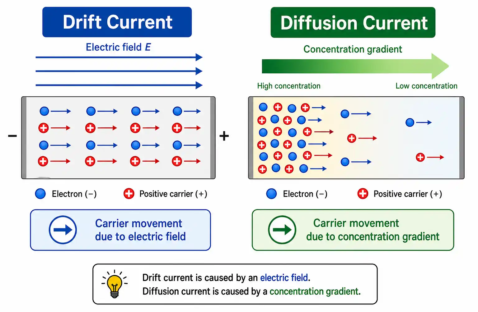
Diffusion current happens due to concentration gradients. When there's a difference in carrier concentration between two regions, carriers naturally move from high-concentration areas to low-concentration areas. This is similar to how perfume spreads across a room—no external force is needed, just the natural tendency toward equilibrium.
Both mechanisms can occur simultaneously in a semiconductor device, and their combined effect determines the total current flow. Understanding when each dominates is crucial for device design and analysis.
2. The Physics Behind Drift Current
Drift current is fundamentally about the response of charge carriers to an electric field. When you apply a voltage across a semiconductor, it creates an electric field within the material.
How Carriers Respond to Electric Fields
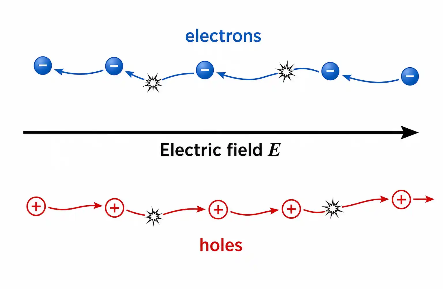
Electrons, being negatively charged, move opposite to the electric field direction. Holes, which represent the absence of electrons and carry positive charge, move in the same direction as the field. This movement isn't instantaneous or uniform—carriers constantly collide with atoms in the crystal lattice.
Carrier Mobility and Drift Velocity
The average velocity that carriers achieve under an electric field is called drift velocity. It's proportional to the electric field strength, and the proportionality constant is called mobility. Mobility depends on the semiconductor material, temperature, and doping concentration.
Higher mobility means carriers can move more easily through the material, resulting in higher drift current for the same electric field. Silicon has different mobility values for electrons and holes, with electrons typically being more mobile.
Scattering Mechanisms
As carriers drift, they scatter off lattice vibrations (phonons) and impurity atoms. This scattering limits how fast carriers can move and is why drift velocity doesn't increase indefinitely with electric field strength. At very high fields, carriers reach a saturation velocity.
3. Understanding Diffusion Current Fundamentals
Diffusion is a natural process driven by concentration gradients, and it occurs in semiconductors just as it does in gases and liquids.
Concentration Gradients in Semiconductors
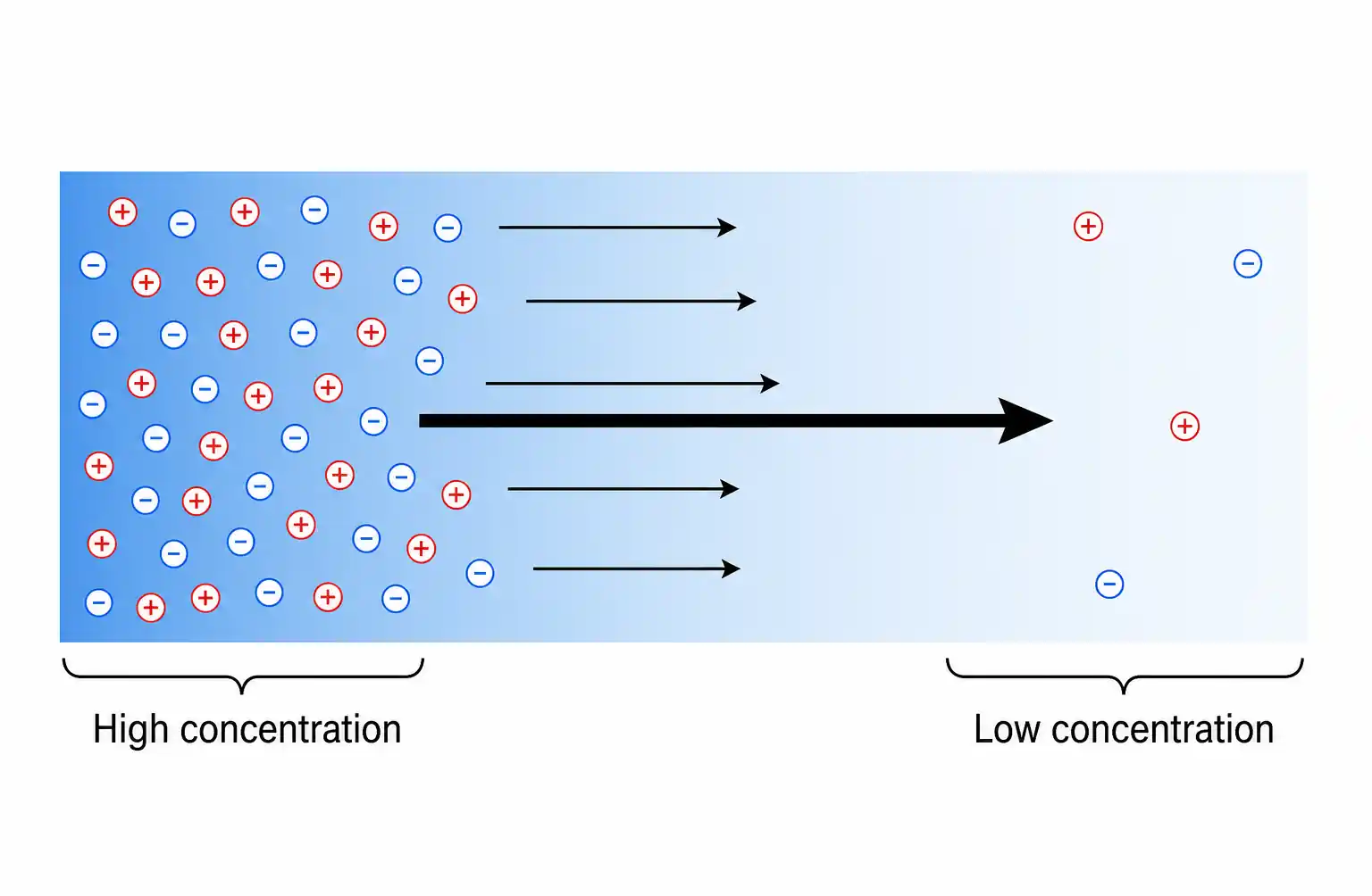
When carrier concentration varies spatially in a semiconductor, a concentration gradient exists. This gradient creates a driving force for carrier movement, even without an electric field.
Fick's Law and Carrier Diffusion
The diffusion process follows Fick's law of diffusion. Carriers move from regions of high concentration to regions of low concentration, attempting to equalize the distribution. The rate of diffusion depends on the steepness of the concentration gradient and a material property called the diffusion coefficient.
Random Thermal Motion
At the microscopic level, diffusion results from the random thermal motion of carriers. Even in equilibrium, carriers are constantly moving in random directions. When there's a concentration gradient, more carriers move from the high-concentration side than from the low-concentration side, creating a net current.
The diffusion coefficient is related to mobility through the Einstein relation, connecting the random thermal motion to the organized drift motion under an electric field.
4. Key Differences Between Drift and Diffusion Currents
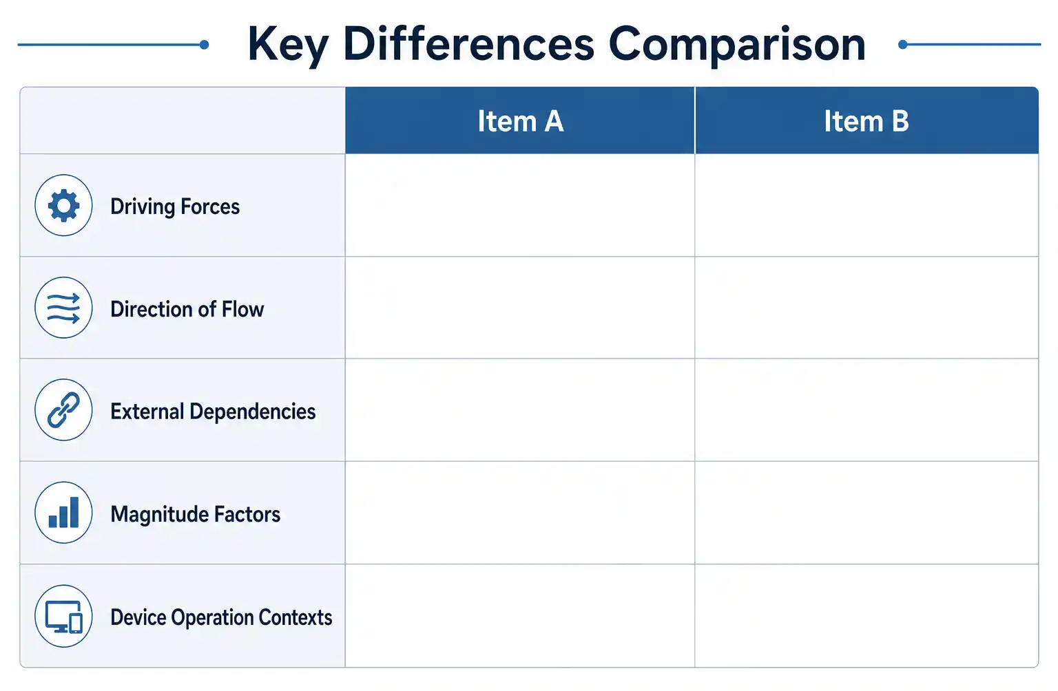
While both contribute to current flow, drift and diffusion currents arise from fundamentally different mechanisms and have distinct characteristics.
Driving Forces
- Drift current: Driven by an external electric field
- Diffusion current: Driven by concentration gradients
Direction of Flow
- Drift current: Direction determined by the electric field and carrier charge
- Diffusion current: Direction determined by the concentration gradient (high to low concentration)
Dependence on External Conditions
Drift current requires an applied voltage or built-in electric field. Diffusion current can occur even without any external voltage, as long as a concentration gradient exists.
Magnitude Factors
Drift current magnitude depends on electric field strength, carrier concentration, and mobility. Diffusion current magnitude depends on the concentration gradient steepness and the diffusion coefficient.
Device Operation Context
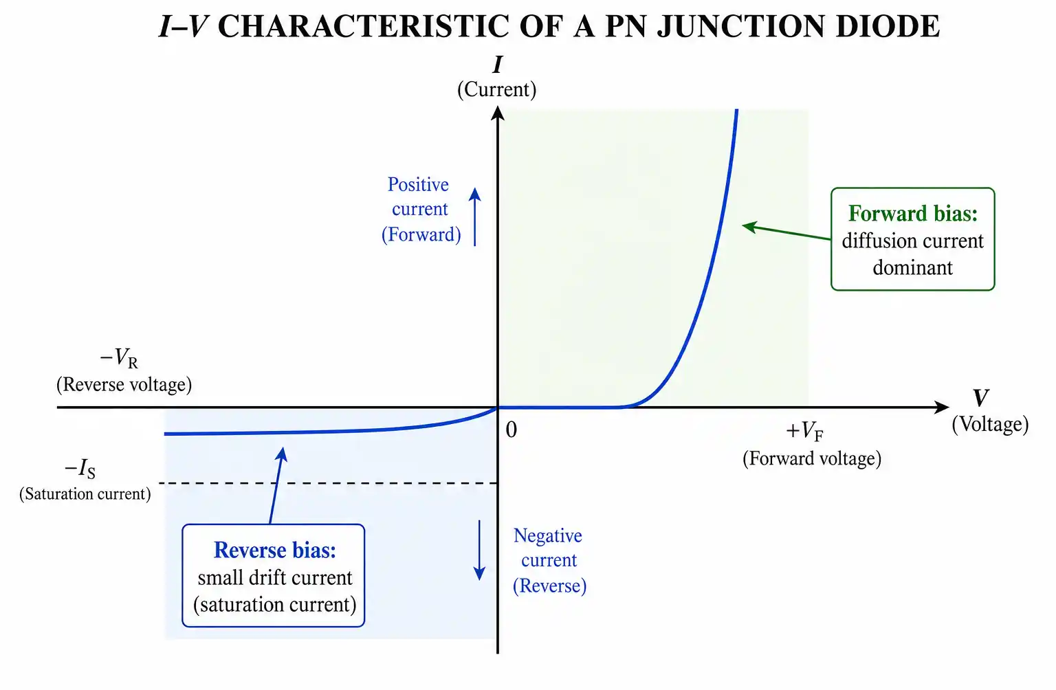
In many devices, both currents flow simultaneously. In a forward-biased PN junction, diffusion current dominates. In a reverse-biased junction, drift current is the primary mechanism. In the depletion region of a PN junction at equilibrium, drift and diffusion currents exactly balance each other.
5. Mathematical Equations for Current Calculations
Understanding the mathematical formulation of these currents is essential for quantitative device analysis.
Drift Current Density Equation
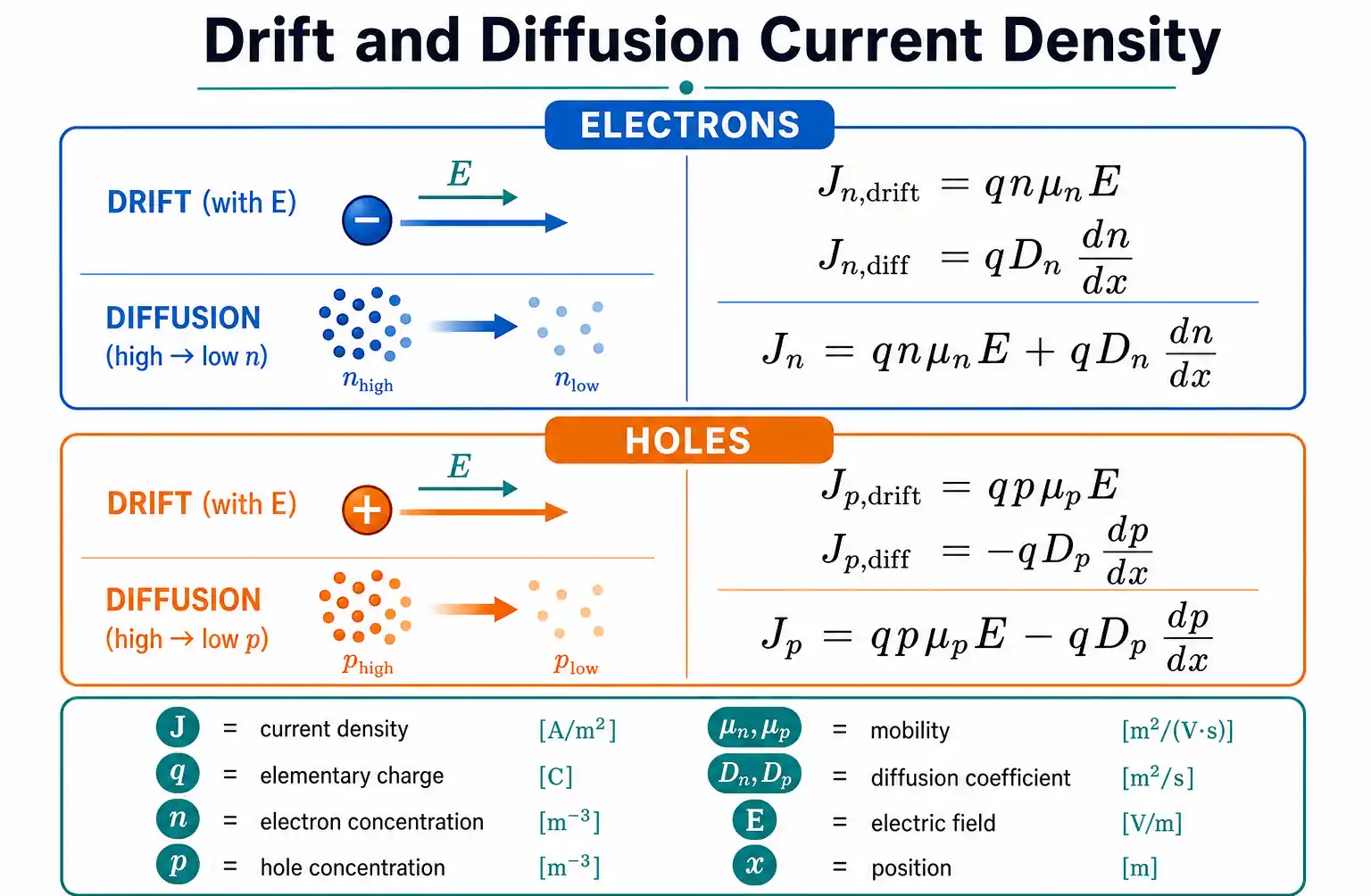
The drift current density for electrons is:
J_drift,n = q × n × μ_n × E
Where:
- J_drift,n = electron drift current density
- q = elementary charge (1.6 × 10⁻¹⁹ C)
- n = electron concentration
- μ_n = electron mobility
- E = electric field strength
For holes, the equation is similar:
J_drift,p = q × p × μ_p × E
Diffusion Current Density Equation
The diffusion current density for electrons is:
J_diff,n = q × D_n × (dn/dx)
Where:
- J_diff,n = electron diffusion current density
- D_n = electron diffusion coefficient
- dn/dx = electron concentration gradient
For holes:
J_diff,p = -q × D_p × (dp/dx)
The negative sign accounts for the fact that holes move in the direction opposite to their concentration gradient when considering conventional current direction.
Total Current Density
The total current density in a semiconductor is the sum of all four components:
J_total = J_drift,n + J_drift,p + J_diff,n + J_diff,p
Einstein Relation
The diffusion coefficient and mobility are related through the Einstein relation:
D/μ = kT/q = V_T
Where:
- k = Boltzmann constant
- T = absolute temperature
- V_T = thermal voltage (approximately 26 mV at room temperature)
This relation is fundamental in semiconductor physics and shows that materials with high mobility also have high diffusion coefficients.
6. How These Currents Work in PN Junctions
The PN junction is the most fundamental semiconductor device structure, and it provides an excellent example of how drift and diffusion currents interact.
Formation of the Depletion Region
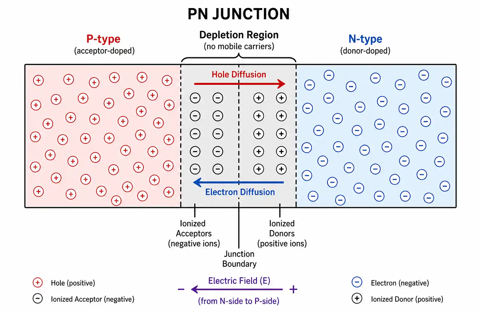
When P-type and N-type semiconductors are joined, electrons from the N-side diffuse to the P-side, and holes from the P-side diffuse to the N-side. This creates a region depleted of mobile carriers near the junction.
Built-in Electric Field
As carriers diffuse across the junction, they leave behind ionized dopant atoms, creating a built-in electric field. This field points from the N-side to the P-side and opposes further diffusion.
Equilibrium Condition
At equilibrium (no external bias), the diffusion current and drift current exactly cancel each other. Carriers still diffuse due to the concentration gradient, but the built-in field creates an equal and opposite drift current. The net current is zero.
Forward Bias Operation
When a forward bias is applied (positive voltage to P-side), the external field opposes the built-in field, reducing the barrier. Diffusion current increases significantly while drift current remains relatively constant. The large diffusion current dominates, allowing substantial current flow.
Reverse Bias Operation
Under reverse bias (positive voltage to N-side), the external field adds to the built-in field, increasing the barrier. Diffusion current becomes negligible, and only a small drift current (saturation current) flows due to minority carriers.
Depletion Region Width
The width of the depletion region changes with bias. Forward bias narrows it, while reverse bias widens it. This affects the electric field strength and the balance between drift and diffusion.
7. Factors Affecting Carrier Transport
Several factors influence how effectively carriers move through semiconductors, affecting both drift and diffusion currents.
Temperature Effects
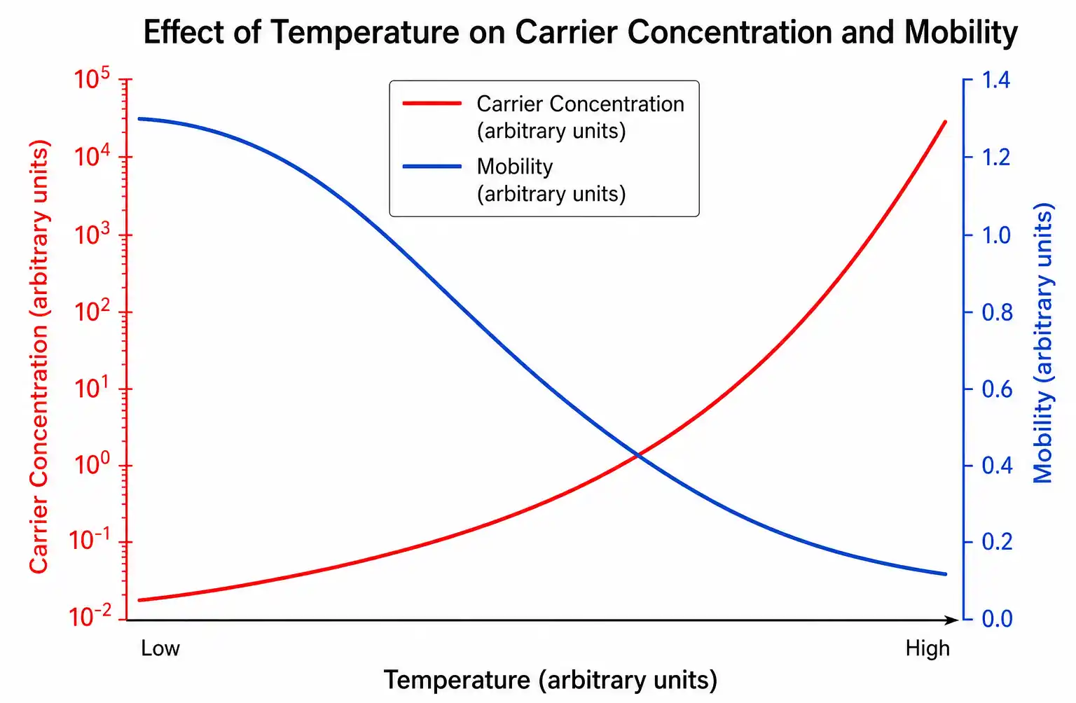
Temperature has a profound impact on carrier transport. Higher temperatures increase thermal energy, which:
- Increases carrier concentration through intrinsic generation
- Increases diffusion coefficients (carriers move faster)
- Decreases mobility (more scattering from lattice vibrations)
The net effect on current depends on which mechanism dominates in a particular device region.
Doping Concentration
Doping level affects carrier transport in multiple ways:
- Higher doping increases majority carrier concentration
- Higher doping decreases mobility due to ionized impurity scattering
- Doping creates concentration gradients that drive diffusion
Electric Field Strength
At low electric fields, drift velocity increases linearly with field strength. At high fields, carriers reach saturation velocity due to increased scattering. This velocity saturation is important in short-channel MOSFETs.
Material Properties
Different semiconductor materials have different intrinsic properties:
- Silicon has moderate mobility and is widely used
- Gallium arsenide has higher electron mobility, useful for high-speed devices
- Silicon carbide has high breakdown field strength, useful for power devices
Crystal Quality and Defects
Crystal defects, dislocations, and impurities create scattering centers that reduce mobility and affect carrier lifetime. High-quality crystals are essential for high-performance devices.
8. Role of Doping in Current Behavior
Doping is the intentional introduction of impurity atoms to control semiconductor properties, and it fundamentally affects both drift and diffusion currents.
N-Type and P-Type Doping
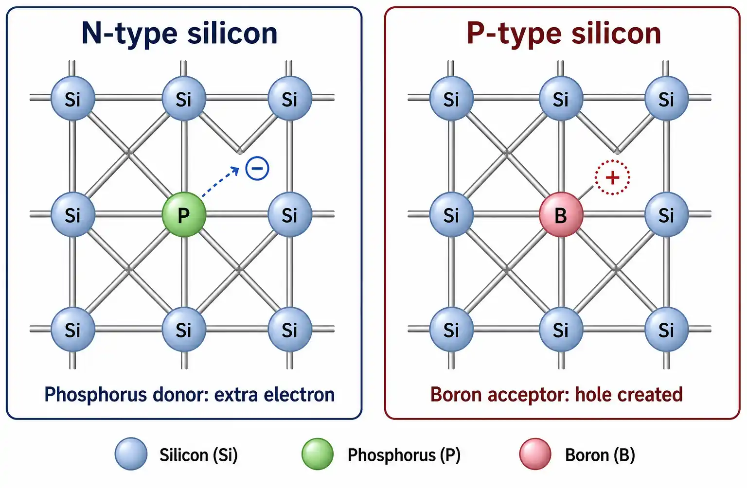
N-type doping introduces donor atoms (like phosphorus in silicon) that provide extra electrons. This increases electron concentration and makes electrons the majority carriers.
P-type doping introduces acceptor atoms (like boron in silicon) that create holes. This increases hole concentration and makes holes the majority carriers.
Impact on Drift Current
Doping directly affects drift current by changing carrier concentration. Higher doping means more carriers available to conduct current under an electric field. However, higher doping also reduces mobility due to increased ionized impurity scattering.
The conductivity (σ) of a semiconductor is:
σ = q(nμ_n + pμ_p)
Doping increases n or p, but decreases μ, so there's an optimal doping level for maximum conductivity.
Impact on Diffusion Current
Doping creates concentration gradients, especially at junctions between differently doped regions. These gradients drive diffusion currents. The steeper the gradient, the larger the diffusion current.
In a PN junction, the doping levels on both sides determine the built-in potential and the width of the depletion region, which in turn affect the balance between drift and diffusion.
Graded vs. Abrupt Junctions
Abrupt junctions have a sharp transition in doping concentration, creating a steep gradient and strong diffusion current.
Graded junctions have a gradual transition, resulting in a more distributed electric field and different current characteristics.
Heavy Doping Effects
At very high doping levels (>10¹⁸ cm⁻³), several effects occur:
- Bandgap narrowing
- Degeneracy (Fermi level enters conduction or valence band)
- Reduced mobility due to heavy impurity scattering
- Modified diffusion behavior
9. Applications in Semiconductor Devices
Understanding drift and diffusion currents is essential for analyzing and designing various semiconductor devices.
Diodes
In diodes, the interplay between drift and diffusion currents determines the I-V characteristics. Forward current is primarily diffusion current, while reverse current is drift current of minority carriers.
Bipolar Junction Transistors (BJTs)
BJTs rely heavily on diffusion current. When the base-emitter junction is forward biased, minority carriers are injected into the base and diffuse across it. The base width must be smaller than the diffusion length for efficient transistor action.
MOSFETs
In MOSFETs, drift current dominates in the channel. The gate voltage creates an electric field that forms an inversion layer, and the drain-source voltage drives drift current through this channel. Short-channel effects involve velocity saturation of drifting carriers.
Solar Cells
Solar cells generate current when photons create electron-hole pairs. These carriers separate due to the built-in field (drift) and concentration gradients (diffusion). The balance between drift and diffusion determines the open-circuit voltage and short-circuit current.
LEDs and Laser Diodes
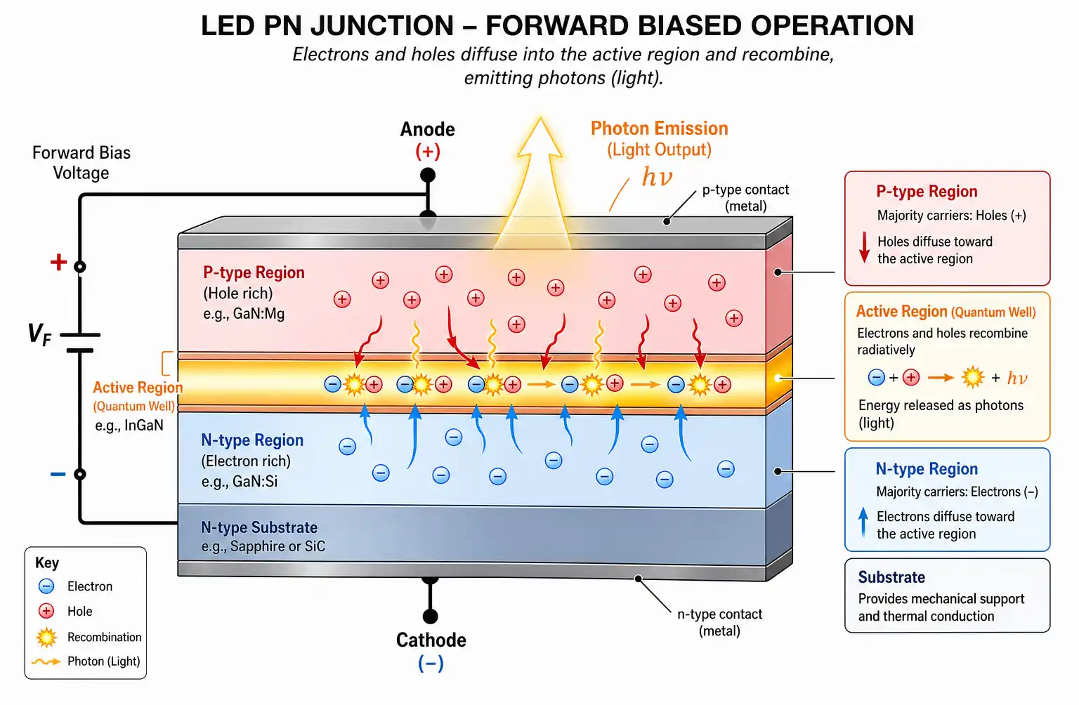
In light-emitting devices, forward bias drives diffusion current across the junction. Electrons and holes recombine in the active region, emitting photons. The efficiency depends on how effectively carriers diffuse to the recombination region.
Photodetectors
Photodetectors operate under reverse bias. Photogenerated carriers are swept across the depletion region by drift current, creating a photocurrent. Fast response requires efficient drift transport.
Thyristors and Power Devices
Power devices often involve multiple junctions and complex interactions between drift and diffusion. Understanding carrier transport is crucial for optimizing switching speed and power handling.
10. Temperature Effects on Drift and Diffusion
Temperature is a critical parameter that affects semiconductor behavior, influencing both types of current in different ways.
Intrinsic Carrier Concentration
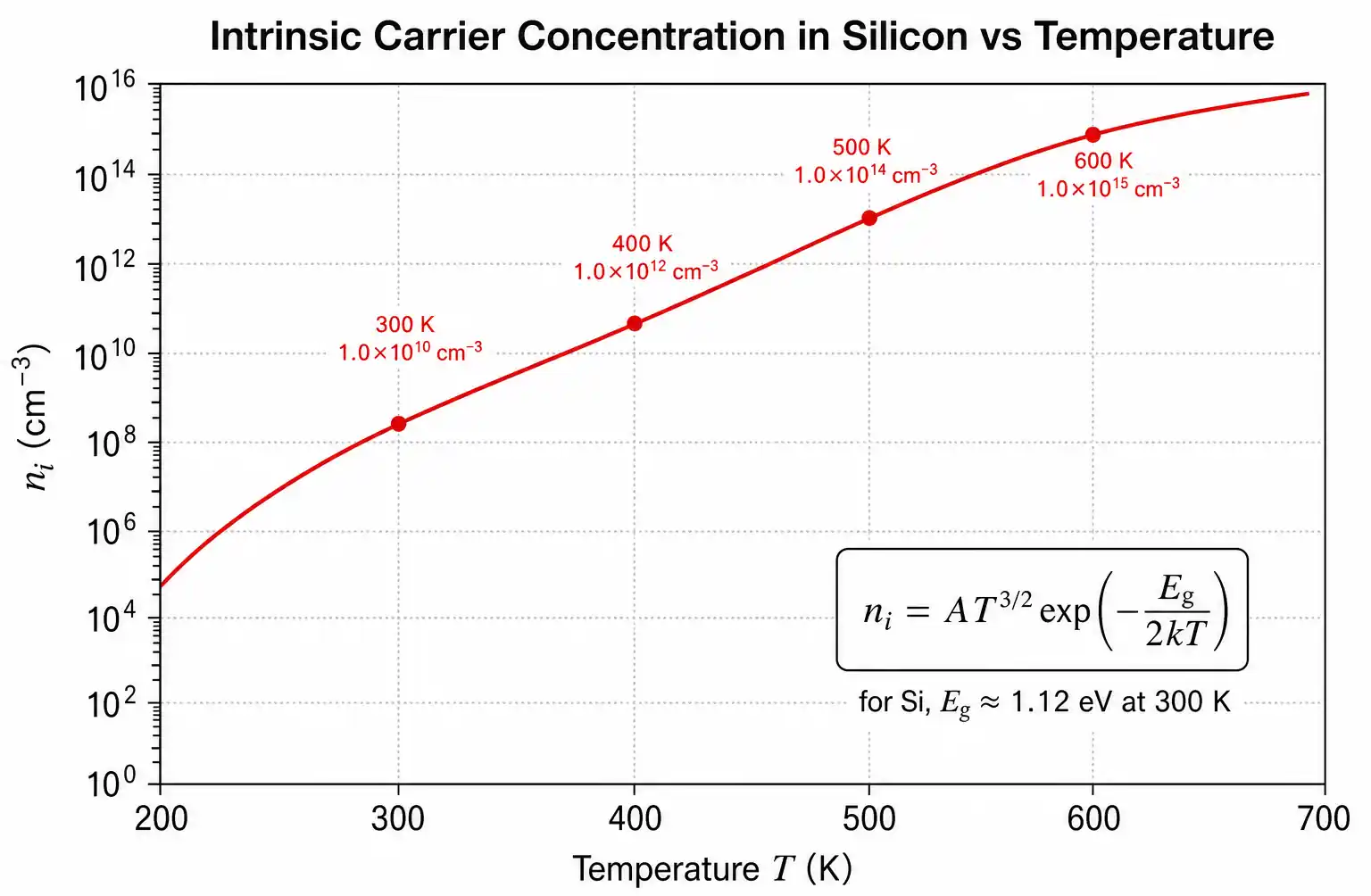
Temperature exponentially increases intrinsic carrier concentration according to:
n_i ∝ T^(3/2) × exp(-E_g/2kT)
Where E_g is the bandgap energy. This dramatically affects minority carrier concentrations and diffusion currents.
Mobility Temperature Dependence
Mobility decreases with increasing temperature due to enhanced phonon scattering. The relationship is approximately:
μ ∝ T^(-3/2) (for lattice scattering)
At low temperatures or high doping, ionized impurity scattering dominates, and mobility increases with temperature.
Diffusion Coefficient Changes
Since diffusion coefficient is related to mobility through the Einstein relation, and both depend on temperature, the diffusion coefficient's temperature dependence is complex. The thermal voltage V_T increases linearly with temperature, affecting the D/μ ratio.
Device Performance Implications
Temperature affects device performance in several ways:
- Leakage current increases exponentially with temperature
- Threshold voltage in MOSFETs decreases with temperature
- Forward voltage drop in diodes decreases with temperature
- Switching speed can be affected by mobility changes
Thermal Runaway
In power devices, increased temperature leads to increased current, which generates more heat. This positive feedback can cause thermal runaway if not properly managed through heat sinking and current limiting.
11. Common Misconceptions and FAQs
Let's address some common questions and misconceptions about drift and diffusion currents.
Can diffusion current exist without an electric field?
Yes, absolutely. Diffusion current is driven by concentration gradients, not electric fields. However, in many practical situations, diffusion creates charge separation, which generates an electric field that opposes further diffusion.
Do drift and diffusion always oppose each other?
Not always. In some device regions, they can flow in the same direction. For example, in the neutral regions of a forward-biased PN junction, both drift and diffusion of minority carriers flow toward the junction.
Which current is larger in a forward-biased diode?
Diffusion current dominates in a forward-biased diode. The forward bias reduces the barrier, allowing majority carriers to diffuse across the junction in large numbers.
Why is drift current called "drift"?
The term "drift" refers to the slow, average motion of carriers in response to an electric field, superimposed on their much faster random thermal motion. Carriers "drift" in the field direction while bouncing around randomly.
How do you measure drift and diffusion currents separately?
In practice, you measure total current. Separating drift and diffusion components requires modeling and analysis based on device structure, bias conditions, and carrier profiles. Techniques like Hall effect measurements can provide information about carrier mobility and concentration.
Is diffusion current always present in semiconductors?
Diffusion current only flows when there's a concentration gradient. In a uniformly doped semiconductor in equilibrium, there's no concentration gradient and no diffusion current.
What happens at very high electric fields?
At very high fields, drift velocity saturates due to increased scattering. Carriers can also gain enough energy to cause impact ionization, creating additional electron-hole pairs. This can lead to avalanche breakdown.
How does carrier lifetime affect these currents?
Carrier lifetime affects how far carriers can diffuse before recombining (diffusion length). Longer lifetime means carriers can travel farther, which is important for device performance, especially in BJTs and solar cells.
Conclusion
Drift and diffusion currents are fundamental to semiconductor device operation. Drift current, driven by electric fields, and diffusion current, driven by concentration gradients, work together to enable the functionality of diodes, transistors, solar cells, and countless other devices.
Understanding these mechanisms provides insight into device behavior, helps in troubleshooting performance issues, and guides the design of new semiconductor technologies. As devices continue to shrink and new materials are explored, the principles of carrier transport remain central to semiconductor physics and engineering.
Whether you're a student learning the basics or an engineer optimizing device performance, a solid grasp of drift and diffusion currents is essential for success in the semiconductor field.