



GaN vs SiC Power Devices: Next-Generation Power Electronics
Wide bandgap (WBG) semiconductors are transforming power electronics across electric vehicles, AI data centers, and renewable energy systems. By 2026, SiC and GaN adoption is accelerating with the power SiC market projected to reach $10 billion. These materials enable devices that operate at higher voltages, temperatures, and switching frequencies than silicon—driving efficiency gains of 15-30% in power conversion systems.
If you need to select power devices for high-performance applications, then you must understand the fundamental differences between gallium nitride (GaN) and silicon carbide (SiC). This comparison guide draws from industry deployment data across automotive, data center, and industrial markets to help you make informed sourcing decisions.
Table of Contents
- Understanding Wide Bandgap Power Devices
- Material Properties: GaN vs SiC
- Switching Performance Comparison
- Thermal Management Characteristics
- Voltage and Power Ratings
- Application Domains
- Cost Analysis and Market Trends
- Selection Criteria for Your Application
- FAQs
- Conclusion
Understanding Wide Bandgap Power Devices
Wide bandgap semiconductors possess bandgap energies significantly higher than silicon's 1.1 eV. GaN features a 3.4 eV bandgap while SiC reaches 3.3 eV for its 4H polytype. This property enables operation at higher voltages and temperatures with lower conduction losses compared to silicon MOSFETs and IGBTs.
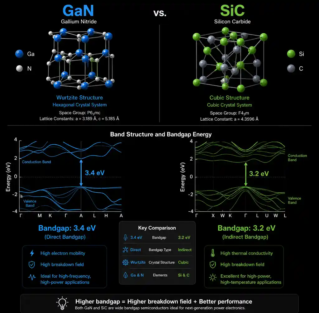 GaN vs SiC crystal structure comparison showing bandgap energy differences
The shift to WBG devices addresses critical limitations in silicon-based power electronics. Silicon devices struggle above 600V and 150°C, requiring oversized heatsinks and limiting switching frequencies to below 100 kHz. GaN and SiC overcome these constraints through superior material characteristics, enabling more efficient power conversion across demanding applications.
You can source both GaN HEMTs (high electron mobility transistors) and SiC MOSFETs from authorized distributors for applications ranging from USB-C fast chargers to 800V EV inverters. Understanding which technology fits your voltage class, frequency requirements, and thermal environment determines system performance and reliability.
The physics behind wide bandgap performance lies in the relationship between bandgap energy and several key device characteristics. A larger bandgap directly translates to higher breakdown electric field strength—GaN achieves 3.3 MV/cm compared to silicon's 0.3 MV/cm. This ten-fold improvement means you can build devices with thinner drift regions for the same voltage rating, dramatically reducing on-resistance (RDS(on)) and conduction losses.
Material Properties: GaN vs SiC
The fundamental material characteristics of GaN and SiC create distinct performance profiles that guide application selection.
| Property | Silicon (Si) | Gallium Nitride (GaN) | Silicon Carbide (SiC) | Engineering Impact |
|---|---|---|---|---|
| Bandgap Energy | 1.1 eV | 3.4 eV | 3.3 eV | Higher voltage capability |
| Critical Field | 0.3 MV/cm | 3.3 MV/cm | 2.5 MV/cm | Thinner drift regions |
| Electron Mobility | 1400 cm²/V·s | 2000 cm²/V·s | 950 cm²/V·s | GaN: faster switching |
| Thermal Conductivity | 1.5 W/cm·K | 1.3 W/cm·K | 4.9 W/cm·K | SiC: superior heat removal |
| Saturation Velocity | 1.0×10⁷ cm/s | 2.5×10⁷ cm/s | 2.0×10⁷ cm/s | Determines max frequency |
Electron mobility determines how quickly carriers respond to applied voltage. GaN's higher mobility (2000 cm²/V·s) compared to SiC (950 cm²/V·s) enables lower on-resistance at the same voltage rating, particularly beneficial below 650V where mobility dominates over drift region thickness. This advantage makes GaN the preferred choice for high-frequency, low-to-medium voltage applications.
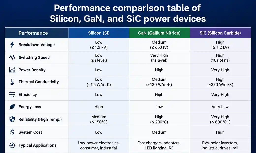 Performance comparison table of Silicon, GaN, and SiC power devices
Thermal conductivity becomes critical for high-power density applications. SiC's exceptional 4.9 W/cm·K—nearly four times that of GaN—allows more efficient heat extraction from the die to the package and ultimately to the heatsink. For applications exceeding 10 kW where junction temperature management is paramount, SiC's thermal advantage outweighs GaN's electrical benefits.
Critical electric field strength determines how much voltage the semiconductor can block per unit thickness. Both GaN and SiC exceed silicon by factors of 8-10×, but this advantage manifests differently in device structures. GaN typically uses lateral HEMT structures on silicon or SiC substrates, while SiC employs vertical MOSFET designs similar to silicon power devices.
The substrate choice further differentiates these technologies. GaN devices commonly use silicon substrates (GaN-on-Si) for cost reasons, though GaN-on-SiC substrates offer superior thermal performance at premium pricing. SiC devices use native SiC substrates, eliminating lattice mismatch issues but driving higher wafer costs—SiC wafers cost 5-10× more than silicon wafers of equivalent diameter.
Switching Performance Comparison
Switching speed directly impacts efficiency, electromagnetic interference (EMI), and passive component sizing. The combination of low gate charge, small output capacitance, and high electron mobility gives WBG devices significant advantages over silicon.
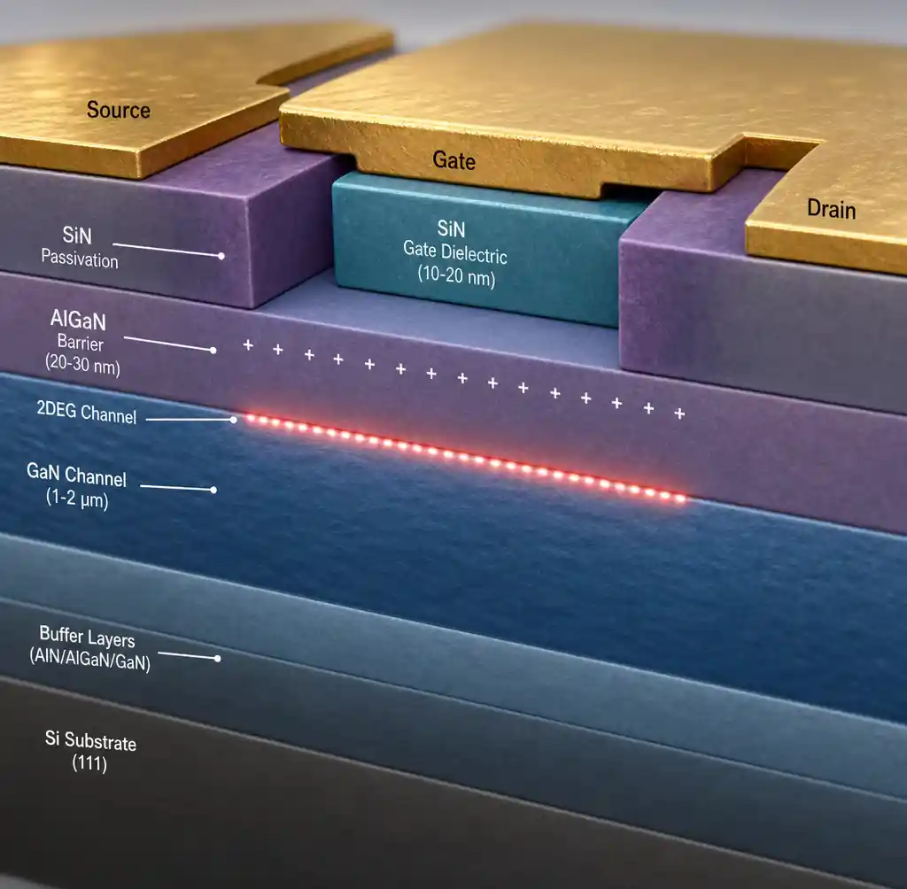 GaN HEMT cross-sectional structure showing 2DEG channel formation
Turn-on and turn-off times measure how quickly the device transitions between blocking and conducting states. GaN HEMTs achieve turn-on times below 10 nanoseconds, while SiC MOSFETs typically range from 15-30 ns. For context, silicon superjunction MOSFETs require 50-100 ns, and IGBTs need 100-300 ns. Faster switching reduces transition losses, which dominate total switching loss at frequencies above 100 kHz.
The gate charge (Qg) required to turn the device on represents energy drawn from the gate driver every switching cycle. Lower Qg reduces gate drive loss and enables higher frequency operation. GaN HEMTs typically feature Qg values 5-10× lower than equivalent-voltage silicon MOSFETs, contributing to their suitability for multi-MHz switching.
Output capacitance (Coss) and its voltage dependence affect both turn-off loss and high-frequency performance. When the device turns off, energy stored in Coss dissipates as heat. GaN devices exhibit lower Coss and more linear voltage dependence compared to silicon superjunction MOSFETs, whose highly non-linear Coss complicates loss calculations. SiC MOSFETs fall between GaN and silicon in terms of Coss magnitude and linearity.
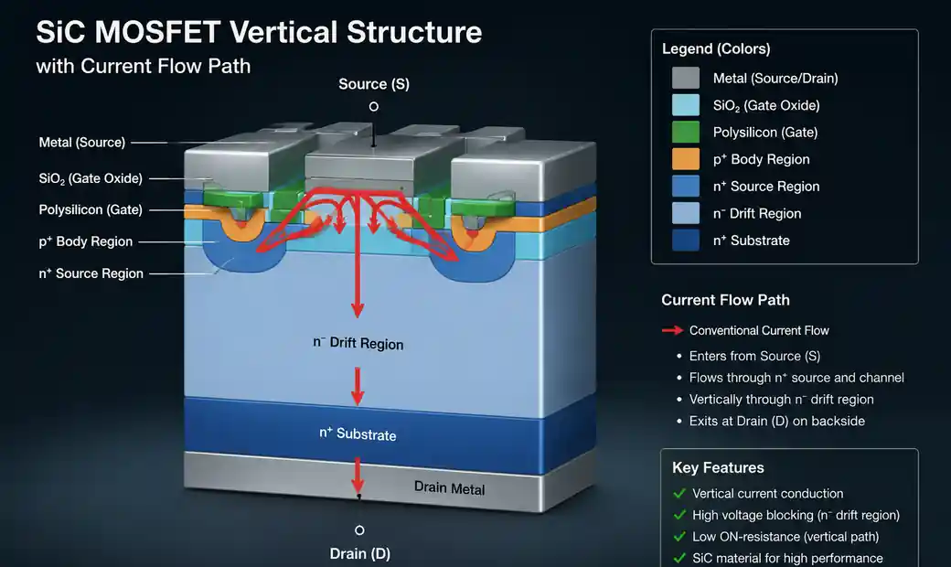 SiC MOSFET vertical device structure with current flow path
These switching characteristics enable dramatically higher switching frequencies. Silicon-based converters typically operate at 50-150 kHz, constrained by switching losses and thermal management. GaN converters routinely switch at 500 kHz to 2 MHz, with some designs exceeding 10 MHz. This frequency increase shrinks magnetic components—a 500 kHz inductor occupies roughly one-third the volume of a 150 kHz inductor for the same power level.
However, faster switching introduces challenges. Parasitic inductance in the power loop becomes more critical as dI/dt increases. PCB layout that works acceptably for 100 kHz silicon designs will cause severe ringing and EMI problems at 1 MHz with GaN. You must minimize loop areas, use multilayer boards with dedicated power planes, and carefully select low-inductance packages. SiC's moderately faster switching (compared to silicon) offers a middle ground—significant efficiency gains without the extreme layout sensitivity of GaN.
Thermal Management Characteristics
Junction temperature capability and thermal resistance determine how much power you can extract from a given package size. WBG devices push both boundaries compared to silicon.
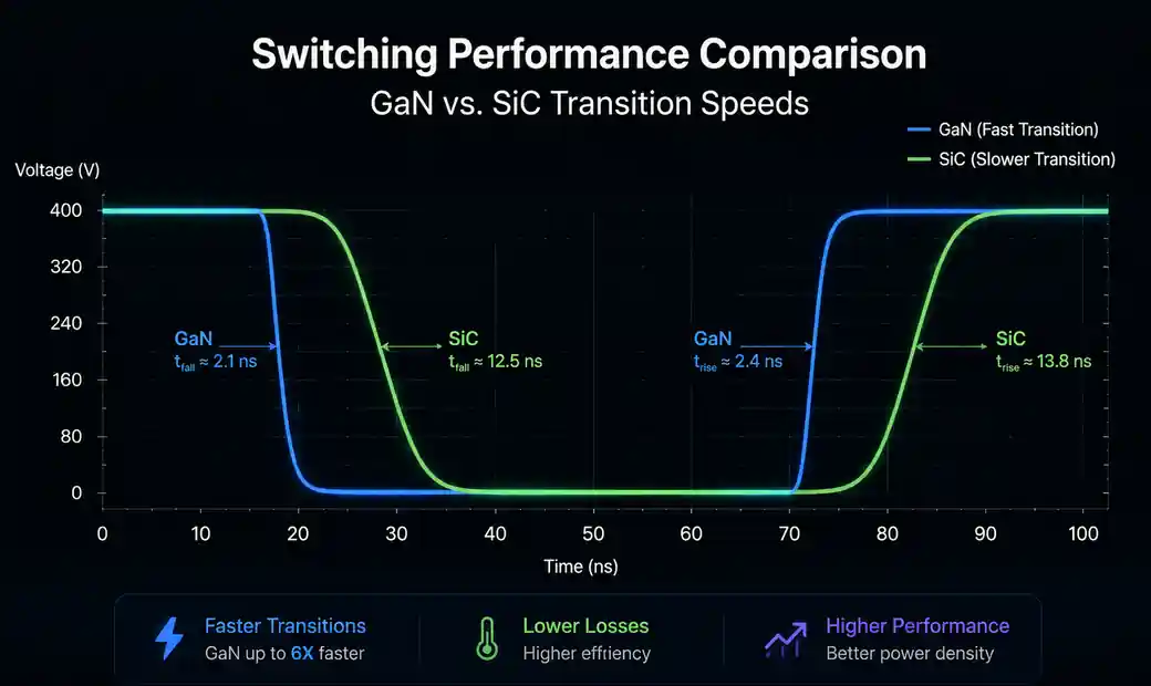 Switching waveform comparison showing GaN vs SiC transition speeds
Maximum junction temperature specifies the highest sustained die temperature. Silicon power devices typically limit Tj,max to 150°C, with some automotive-grade parts rated to 175°C. SiC devices commonly operate at 175-200°C, with emerging designs targeting 250°C for extreme environments. GaN devices typically rate to 150-175°C, constrained more by packaging materials than the GaN material itself.
Higher junction temperature tolerance translates directly to system benefits. For a given cooling solution, you can either extract more power (increasing power density) or reduce heatsink size and cost (maintaining power but improving form factor). In electric vehicle traction inverters, SiC's 175-200°C capability enables cooler designs that integrate directly with the motor housing, eliminating separate inverter enclosures.
Thermal resistance (Rθ,JC, junction-to-case) characterizes heat flow from the die through the package. SiC's superior thermal conductivity yields Rθ,JC values 20-40% lower than silicon devices in similar packages. This advantage compounds with higher Tj,max—you can tolerate both higher die temperature and more efficient heat extraction.
Temperature coefficient of on-resistance differs between technologies. Silicon and SiC MOSFETs exhibit positive temperature coefficients—RDS(on) increases roughly 0.5-0.7%/°C. This characteristic promotes current sharing when paralleling devices, since hotter dies conduct less current and self-balance. GaN HEMTs show weaker temperature dependence, complicating parallel operation but enabling more stable performance across temperature.
Thermal cycling reliability also varies. SiC's thermal expansion coefficient more closely matches common substrate materials (copper, aluminum nitride) compared to GaN-on-Si, where the large silicon/GaN mismatch creates mechanical stress during temperature cycling. For applications with frequent thermal cycles—automotive, solar inverters—SiC demonstrates superior long-term reliability.
Voltage and Power Ratings
Commercial device availability and performance optimization differ significantly across voltage classes, creating natural application domains for each technology.
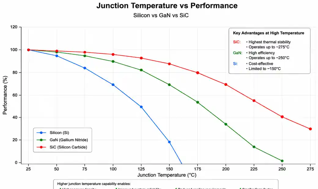 Junction temperature vs performance graph for Silicon, GaN, and SiC
GaN dominates below 650V, where its superior electron mobility translates to lowest RDS(on) per unit area. The sweet spot spans 40-650V, covering USB Power Delivery chargers (20-100V), 48V data center distribution (60-100V), server power supplies (400V), and residential solar microinverters (300-400V). GaN devices in this range offer specific on-resistance (RDS(on) × area) 3-5× better than silicon.
You can source 100V GaN devices with RDS(on) below 10 mΩ in compact DFN packages suitable for phone chargers exceeding 100W in volumes under 20 cm³. Comparable silicon devices require 2-3× larger die area and packages, limiting power density. At 650V, GaN achieves RDS(on) around 50-100 mΩ, enabling kilowatt-scale PFC stages and motor drives with drastically reduced heatsinks.
SiC excels above 650V, where voltage blocking requirements favor its vertical structure and superior thermal performance compensates for lower mobility. Commercial SiC MOSFETs span 650V to 3.3 kV, with research devices exceeding 10 kV. The automotive 800V battery architecture—rapidly becoming standard for premium EVs—drives massive demand for 1200V SiC devices.
At 1200V, SiC MOSFETs achieve RDS(on) around 10-40 mΩ depending on current rating, roughly 3× better than silicon IGBTs at equivalent ratings while switching 5-10× faster. This combination enables 800V traction inverters with 98-99% efficiency and power densities exceeding 30 kW/L—double that of silicon-based 400V systems. Solar inverters similarly benefit, with string inverters using 1500V SiC devices achieving >99% peak efficiency.
Higher voltage SiC devices target industrial and utility applications. The 3.3 kV class serves medium-voltage drives, traction systems, and grid-tied inverters. While these devices currently cost substantially more than IGBTs, their switching speed enables topologies (like multi-level converters at higher switching frequencies) that reduce transformer and filter costs enough to justify the semiconductor premium.
Power scaling follows different paths. GaN devices scale well to medium power (10-20 kW) by paralleling multiple dies in advanced packages. Beyond 20 kW, the lateral structure and thermal limits become constraining. SiC scales naturally to very high power through larger die sizes and module configurations—single SiC modules exceed 500 kW, with parallel configurations reaching multi-MW power levels for traction and utility applications.
Application Domains
Market deployment patterns reveal where each technology delivers optimal cost-performance trade-offs based on voltage, power, frequency, and thermal requirements.
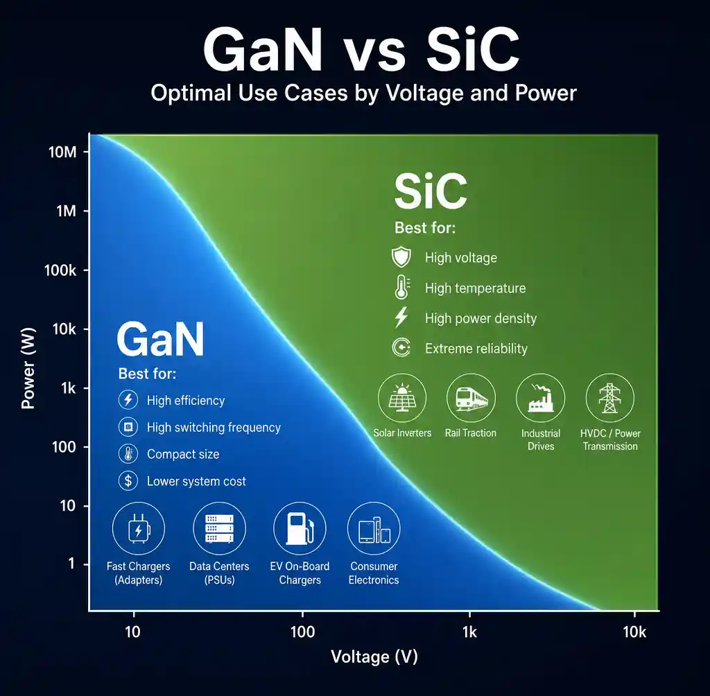 Application matrix showing GaN vs SiC optimal use cases by voltage and power
GaN-optimized applications share common characteristics: medium voltage (40-650V), high switching frequency (>500 kHz), space constraints favoring small magnetics, and power levels from tens of watts to roughly 10 kW.
Consumer and mobile power: USB-C PD chargers represent GaN's highest-volume application, with devices switching at 1-2 MHz enabling chargers under 1 cm³/W power density. Wireless charging transmitters, laptop adapters, and smartphone fast chargers leverage GaN's combination of efficiency (>95%) and density. Major brands including Apple, Samsung, and Anker have adopted GaN chargers across product lines.
Data center power delivery: The shift from 12V to 48V distribution creates ideal conditions for GaN adoption. 48V-to-point-of-load (PoL) converters step down to 1V rails for CPUs and GPUs, requiring extreme current delivery (>500A) with minimal loss. GaN devices switching above 500 kHz enable planar magnetics integration and power module densities exceeding 1 kW/in³. Google and Microsoft data centers have deployed 48V architectures specifically to exploit GaN advantages.
Residential solar and storage: Microinverters (200-400W per panel) and residential battery inverters (3-10 kW) operate at 300-400V DC bus voltages squarely in GaN's sweet spot. Higher switching frequencies reduce magnetics costs and enable single-phase operation without bulky electrolytic capacitors. Enphase and SolarEdge have integrated GaN into microinverter platforms, achieving >97% CEC-weighted efficiency in compact, fan-less enclosures.
SiC-optimized applications require high voltage (>650V), high power (>10 kW), and can leverage SiC's thermal capabilities even at moderate switching frequencies (20-100 kHz).
Electric vehicle powertrains: The 800V battery architecture demands 1200V devices to maintain voltage margins during regenerative braking. SiC-based traction inverters achieve 98-99% efficiency across the operating map, extending range by 5-8% compared to silicon IGBT systems while halving inverter mass and volume. Tesla's Model 3, Porsche Taycan, and most 2026 premium EVs use SiC inverters. Module suppliers including Infineon, Wolfspeed, and ON Semiconductor project EV SiC content exceeding $500 per vehicle by 2028.
Onboard chargers (OBC) and DC fast charging: 11-22 kW onboard chargers must boost 400V battery voltage for unity power factor AC input, requiring 1200V switches for both PFC and DC-DC stages. SiC enables smaller, lighter, and more efficient OBCs—critical for EVs where every kilogram affects range. DC fast chargers (50-350 kW) similarly rely on SiC for the AC-DC rectifier stage and DC-DC output converters, achieving >96% end-to-end efficiency.
Industrial motor drives and traction: Variable frequency drives (VFDs) for industrial motors and rail traction systems traditionally use IGBTs. SiC enables both higher efficiency (reducing operating costs) and higher switching frequency (reducing motor torque ripple and acoustic noise). Medium-voltage drives (2.3-4.16 kV) benefit especially from 3.3 kV SiC devices, enabling two-level topologies that would require complex multi-level designs with IGBTs.
Renewable energy inverters: Utility-scale solar and wind inverters (1-10 MW) operate at 1000-1500V DC bus voltages, requiring 1700V or 3.3 kV devices. SiC's efficiency advantage—typically 1-2% better than IGBTs—compounds over decades of operation, justifying initial cost premium. Major inverter manufacturers including SMA, Sungrow, and Huawei have adopted SiC across commercial and utility products, with some reporting complete IGBT phase-out in new designs.
Cost Analysis and Market Trends
Device cost, supply chain maturity, and ecosystem support influence technology adoption beyond pure performance metrics.
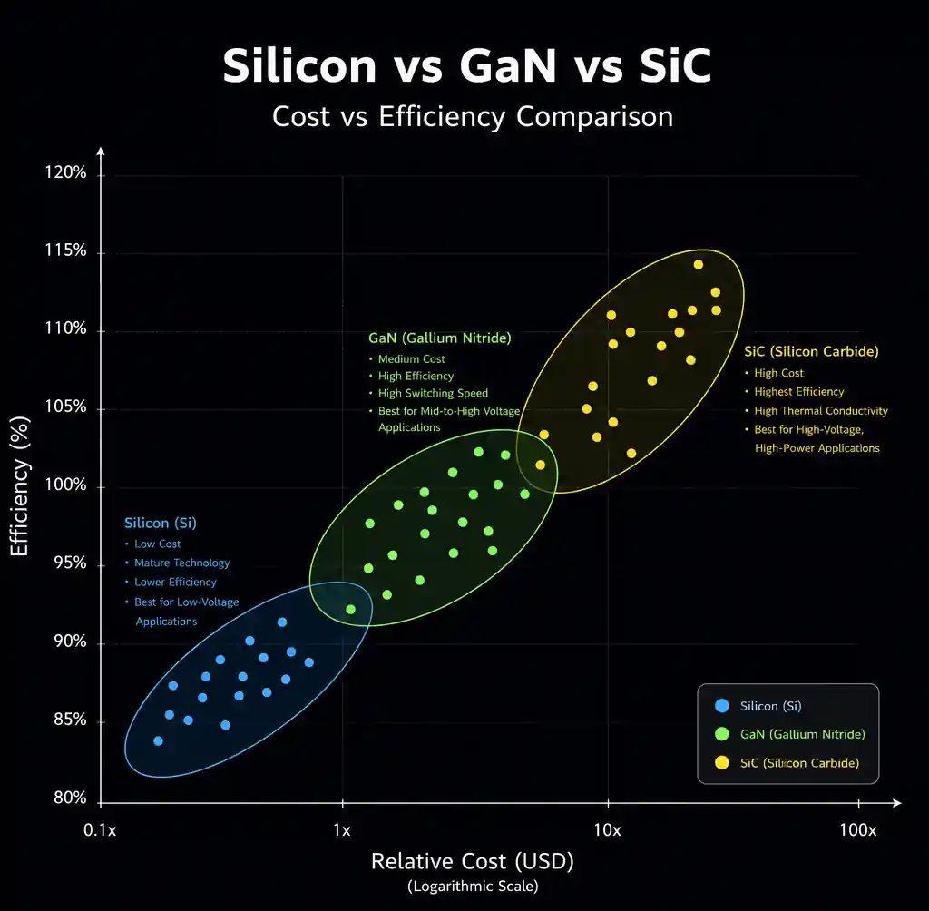 Cost versus efficiency scatter plot comparing Silicon, GaN, and SiC economics
GaN device pricing has dropped dramatically as manufacturing scales. Early GaN devices (2015-2018) commanded 5-10× premiums over silicon equivalents. By 2026, high-volume GaN devices (650V, 15-30A) cost roughly 2-3× comparable silicon MOSFETs. For applications where GaN enables significant system-level savings—smaller magnetics, simpler cooling, higher power density—this premium pays back readily.
Die cost rather than wafer cost drives GaN economics. GaN-on-Si devices use standard 150-200mm silicon wafers processed on existing CMOS equipment, leveraging economies of scale from the semiconductor industry. The challenge lies in device yield and manufacturing maturity. As processes stabilize, GaN pricing should approach silicon more closely, particularly for high-volume consumer applications.
The charging adapter market illustrates cost dynamics. A 65W GaN charger's BOM might include $1.50-2.50 in GaN devices compared to $0.50-1.00 for silicon MOSFETs. However, GaN eliminates roughly $2-3 in magnetics costs (smaller transformer, no PFC inductor) and $0.50 in heatsink costs, yielding net BOM savings despite higher semiconductor cost. Premium pricing ($40-50 vs $15-20 for silicon-based chargers) reflects brand positioning more than component costs.
SiC device pricing remains elevated but follows a predictable decline curve. 1200V SiC MOSFETs cost roughly 3-5× more than equivalently rated IGBTs as of 2026. However, IGBT-based systems require additional components—larger heatsinks, bigger magnetics, auxiliary cooling—that narrow the system-level gap to 1.5-2.5×.
Substrate cost dominates SiC device pricing. SiC wafers cost $1000-3000 per 150mm wafer compared to $50-100 for silicon wafers. Multiple suppliers are scaling to 200mm wafers, which should reduce cost per device by 40-50% through improved die yield. Wolfspeed, Rohm, and STMicroelectronics have announced 200mm production capacity ramping through 2027-2028.
Supply security concerns influence procurement decisions. The SiC supply chain remains concentrated, with a handful of suppliers controlling both substrate and device production. Long lead times (20-52 weeks for high-current modules) and allocation constraints persist despite capacity additions. Many EV manufacturers have secured long-term supply agreements or invested directly in SiC producers to guarantee access. GaN faces fewer supply constraints due to silicon substrate availability and broader fab capabilities.
Selection Criteria for Your Application
Choosing between GaN and SiC requires evaluating your specific requirements across multiple dimensions beyond simple voltage and current ratings.
Start with voltage class. Below 650V, GaN typically offers better performance and approaching cost parity. Above 650V, SiC dominates through voltage scaling capabilities and thermal performance. The 600-900V range represents genuine overlap where both technologies compete based on other factors.
Switching frequency requirements guide technology choice within the viable voltage range. If your application benefits from >500 kHz switching—to shrink magnetics, improve transient response, or reduce output filtering—GaN's superior switching speed justifies potential challenges. If 50-200 kHz suffices for your performance targets, SiC delivers excellent efficiency without extreme layout constraints.
Thermal environment and cooling constraints favor different solutions. Ambient temperatures above 85°C or limited cooling airflow benefit from SiC's higher junction temperature rating and superior thermal conductivity. Space-constrained applications where heatsink volume drives product size may accept GaN's higher thermal resistance in exchange for drastically reduced magnetics volume.
Power level and current requirements create practical boundaries. Single-device GaN solutions scale naturally to 20-30A at 650V. Higher currents require paralleling devices or moving to SiC. For >100A requirements, SiC modules offer integrated current sensing, thermal monitoring, and optimized layouts that simplify power stage design.
EMI and layout complexity considerations matter beyond datasheet parameters. GaN's extreme switching speed demands careful PCB design—four-layer boards minimum, dedicated power planes, kelvin source connections, RC snubbers on gates. Teams without extensive high-frequency layout experience may find SiC's more moderate switching speed easier to implement successfully. Conversely, teams targeting maximum power density and possessing layout expertise can fully exploit GaN's advantages.
Supply chain and second-source availability affect production risk. For critical industrial or automotive applications, SiC's broader supplier base (Infineon, Wolfspeed, STMicro, Rohm, ON Semi, Mitsubishi) provides more sourcing options despite overall supply tightness. GaN suppliers have consolidated around fewer vendors (GaN Systems, Transphorm, Navitas, Infineon, Texas Instruments), though most offer broad portfolios within their technology.
FAQs
Can I directly replace silicon MOSFETs with GaN or SiC devices?
No, not without circuit modifications. GaN HEMTs typically require negative gate voltage capability (-10V) and different gate drive timing compared to silicon MOSFETs. SiC MOSFETs need higher gate drive voltage (+15 to +20V vs +10V for silicon) and carefully controlled gate resistance to manage the faster switching. Both require attention to layout parasitics that silicon designs tolerate. Plan for board redesign when migrating to WBG devices.
Why aren't GaN devices available above 650V?
GaN's lateral HEMT structure becomes inefficient at higher voltages. The drift region length scales with voltage, increasing on-resistance and die area. SiC's vertical structure scales more efficiently—current flows perpendicular to the wafer surface, so voltage rating increases by making the drift region thicker rather than wider. Some vendors offer 900V GaN devices, but performance no longer justifies cost compared to SiC alternatives.
Do GaN and SiC devices require special gate drivers?
Yes, optimized gate drivers designed for WBG devices improve performance and reliability. GaN drivers provide fast edge rates (2-5V/ns), negative off-state voltage, and tight control over turn-on/turn-off timing. SiC drivers deliver higher peak current (±5 to ±10A) to rapidly charge/discharge larger gate capacitance and often include active Miller clamp circuits to prevent inadvertent turn-on. Using silicon-optimized drivers with WBG devices typically works but sacrifices performance.
Which technology is better for paralleling devices?
SiC's positive temperature coefficient of RDS(on) makes it inherently better for paralleling—hotter devices conduct less current, promoting even current distribution. GaN's flatter temperature dependence requires more careful matching and thermal design when paralleling. For high-current applications requiring parallel devices, SiC simplifies design and improves reliability.
Conclusion
GaN and SiC power devices represent complementary advances in power electronics rather than competing alternatives. GaN optimizes performance below 650V where high switching frequency and power density matter most—consumer power, data center distribution, and residential energy systems. SiC addresses high-voltage, high-power applications where thermal performance and voltage scaling capabilities prove decisive—electric vehicles, industrial drives, and utility power conversion.
Your application's voltage class provides the primary selection criterion, with switching frequency requirements, thermal environment, and power level refining the choice within the viable range. Both technologies continue rapid development, with costs declining and supply chains maturing. As manufacturing scales and second-source availability improves, WBG device adoption will accelerate across power electronics applications currently served by silicon MOSFETs and IGBTs.
For procurement managers and design engineers planning next-generation products, understanding these fundamental trade-offs enables informed component selection that balances performance, cost, supply security, and design complexity to meet your specific application requirements.