



Power Transistor Thermal Design: SOA, Junction Temperature, and Heat Sink Calculations
Thermal failure accounts for over 55% of power transistor breakdowns in industrial electronics. Understanding Safe Operating Area (SOA), junction temperature management, and heat sink calculations is critical for reliable power circuit design in automotive, industrial automation, and power conversion systems. This guide covers SOA analysis, thermal resistance calculations, derating methods, and heat sink selection.
Table of Contents
- What is Power Transistor Thermal Design?
- Understanding Safe Operating Area (SOA)
- Junction Temperature and Thermal Resistance
- Heat Sink Selection and Calculation
- Temperature Derating for Reliability
- Thermal Runaway Prevention
- Practical Design Examples
- Common Thermal Design Mistakes
- FAQ
- Conclusion
What is Power Transistor Thermal Design?
Power transistor thermal design manages heat dissipation to keep junction temperature within safe limits. Electrical energy converts to heat at the semiconductor junction and must be efficiently conducted through the package, thermal interface material, heat sink, and to ambient air. Every 10°C increase in junction temperature approximately doubles the failure rate.
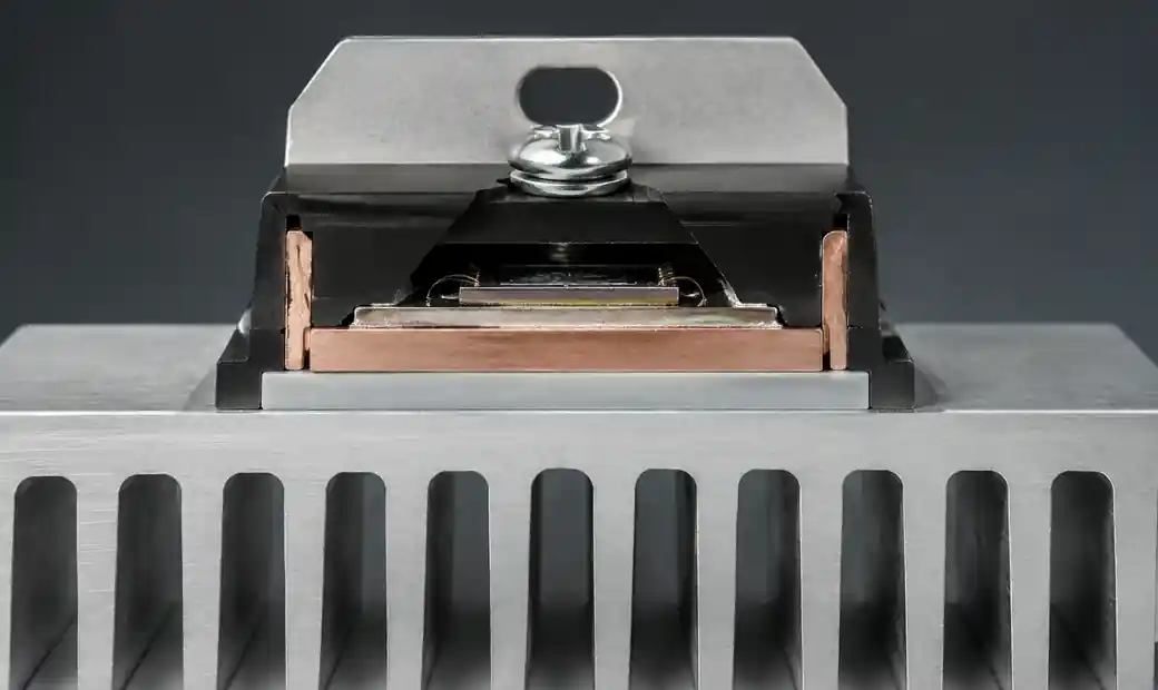 Power transistor thermal management system showing heat flow from junction to ambient
Understanding Safe Operating Area (SOA)
The Safe Operating Area defines voltage and current boundaries for safe transistor operation without damage. SOA curves in datasheets plot drain-source voltage (VDS for MOSFETs) or collector-emitter voltage (VCE for BJTs) against current for multiple pulse durations.
SOA Curve Boundaries
Maximum Current Limit forms the vertical boundary, set by bond wire capacity and package ratings.
Maximum Voltage Limit creates the horizontal boundary at breakdown voltage rating.
Maximum Power Dissipation Line slopes from high current/low voltage toward low current/high voltage, following P = V × I. This boundary shifts with case temperature.
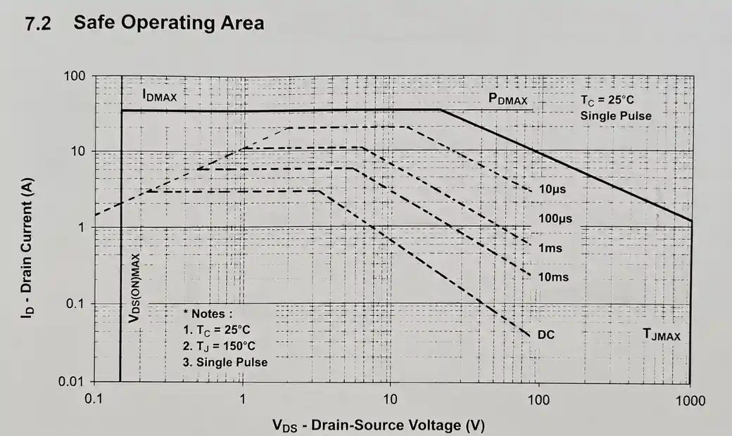 Safe Operating Area SOA curve for power transistor showing voltage and current boundaries
Thermal Limit (Second Breakdown) appears in BJTs as steep negative slope at higher voltages. MOSFETs lack this mechanism due to positive temperature coefficient.
| SOA Boundary | Physical Limit | Design Margin |
|---|---|---|
| Maximum Current | Bond wire/package | 20-30% derating |
| Maximum Voltage | Junction breakdown | 20% derating for inductive loads |
| Power Dissipation | Thermal capacity | TJ < 125°C for reliability |
| Second Breakdown | Current filamentation (BJT only) | Avoid near boundary |
Temperature Derating of SOA
SOA curves at TC = 25°C require proportional derating at elevated temperatures. For TJ(max) = 150°C at TC = 100°C:
I_derated = I_SOA(25°C) × [(TJ(max) - TC) / (TJ(max) - 25°C)]
Junction Temperature and Thermal Resistance
Junction temperature (TJ) is calculated from ambient temperature, power dissipation, and thermal resistance:
TJ = TA + (PD × θJA)
Where θJA = θJC + θCS + θSA
- θJC = Junction-to-case (datasheet parameter, typically 0.3-5°C/W)
- θCS = Case-to-sink (thermal interface, typically 0.2-1°C/W)
- θSA = Sink-to-ambient (heat sink performance, 1-20°C/W)
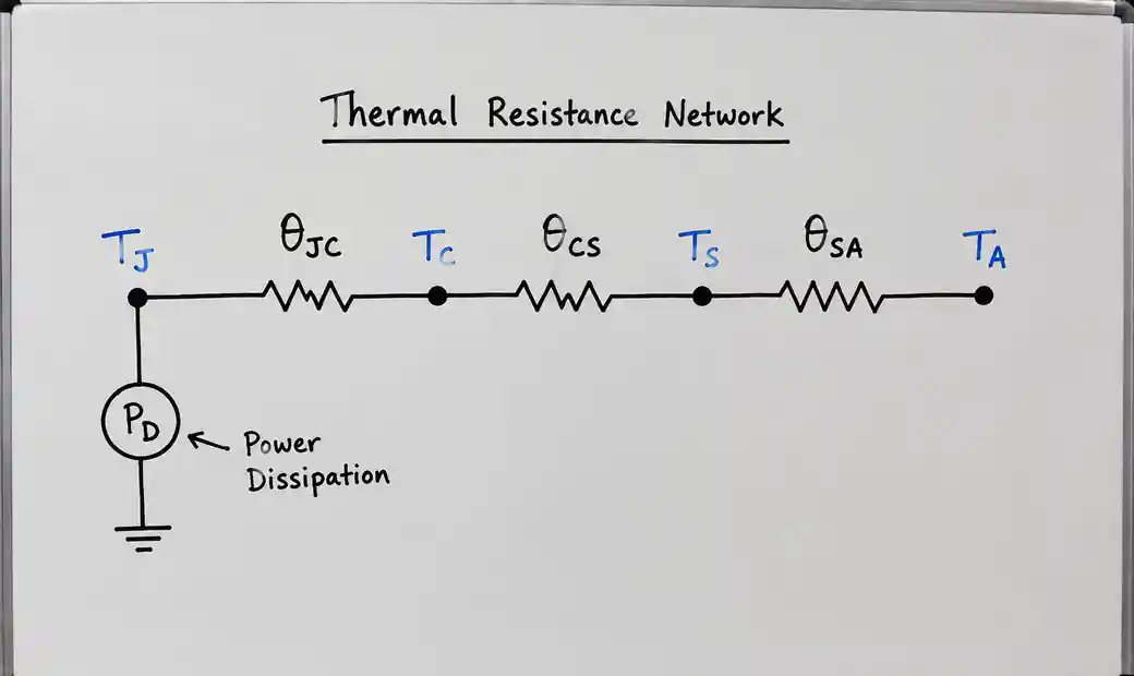 Thermal resistance network model from junction to ambient temperature
Power Dissipation Calculation
For MOSFETs, conduction loss dominates at low frequencies:
PD(conduction) = ID² × RDS(on) × (1 + α × [TJ - 25°C])
Temperature coefficient α (typically 0.004-0.006/°C) accounts for RDS(on) increase. At 150°C, RDS(on) can be 70-80% higher than 25°C values.
Switching losses become significant above 20 kHz:
PD(switching) = (VDS × ID × [tr + tf] × fsw) / 2
| Parameter | Typical Range | Notes |
|---|---|---|
| θJC (TO-220) | 0.5-2°C/W | Device-specific |
| θCS (with grease) | 0.3-0.6°C/W | Thin uniform layer |
| θSA (natural conv.) | 5-15°C/W | Depends on sink size |
| θSA (forced air) | 1-5°C/W | With 100-400 LFM airflow |
Heat Sink Selection and Calculation
Calculate required heat sink thermal resistance from maximum junction temperature:
θSA(required) = [(TJ(max) - TA(max)) / PD(max)] - θJC - θCS
Design for TJ = 125°C rather than absolute maximum (150-175°C) for reliability margin.
Example: MOSFET dissipates 50W at TA = 70°C, θJC = 1.2°C/W, θCS = 0.5°C/W, design TJ = 125°C:
θSA = (125 - 70) / 50 - 1.2 - 0.5 = -0.6°C/W (forced air required)
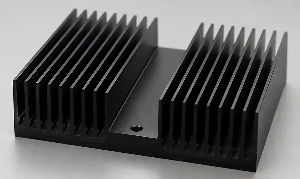 Aluminum extrusion heat sink with fin array for power transistor cooling
Heat Sink Sizing
Natural convection (black anodized aluminum):
- θSA ≈ 10°C/W: Small TO-220 clip-on (~20cm²)
- θSA ≈ 5°C/W: Medium extrusion (~50cm²)
- θSA ≈ 2°C/W: Large heat sink (~150cm²)
Forced air (100-200 LFM) reduces θSA by 40-60%.
Thermal Interface Materials
| Material | θCS (°C/W) | Application |
|---|---|---|
| Thermal grease | 0.3-0.6 | Most common, reapply periodically |
| Thermal pads | 0.5-1.5 | Clean, no maintenance |
| Phase change | 0.3-0.8 | Becomes fluid above 50-60°C |
| Dry contact | 2-10 | Unacceptable for power devices |
Apply thin uniform layer (0.05-0.1mm). Excessive thickness increases resistance.
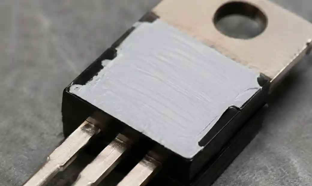 Thermal grease application between transistor case and heat sink surface
Temperature Derating for Reliability
Operating at absolute maximum ratings causes premature failure. Derating extends lifetime by reducing stress on semiconductor materials and package structures.
Derating Guidelines
Military/Aerospace:
- Junction temperature: 75% of TJ(max)
- Power dissipation: 60% of maximum
- Voltage: 80% of breakdown rating
Industrial:
- Junction temperature: 85% of TJ(max)
- Power dissipation: 70% of maximum
- Voltage: 85% of breakdown rating
Operating at 125°C instead of 150°C improves MTTF by 3-5×.
Derating Calculation
For MOSFET rated TJ(max) = 175°C, PD(max) = 300W at TC = 25°C, industrial derating:
TJ(design max) = 175 × 0.85 = 149°C
At TC = 100°C: PD(derated) = 300 × [(149 - 100) / (175 - 25)] = 98W
Thermal Runaway Prevention
Thermal runaway occurs when temperature increase causes more power dissipation in positive feedback. BJTs are susceptible because collector current increases with temperature.
BJT Thermal Runaway: VBE decreases -2mV/°C with temperature. In voltage-biased circuits, this increases base current and collector current, generating more heat.
MOSFET Thermal Stability: RDS(on) increases with temperature (positive coefficient), providing negative feedback. Hotter regions conduct less current, naturally distributing load.
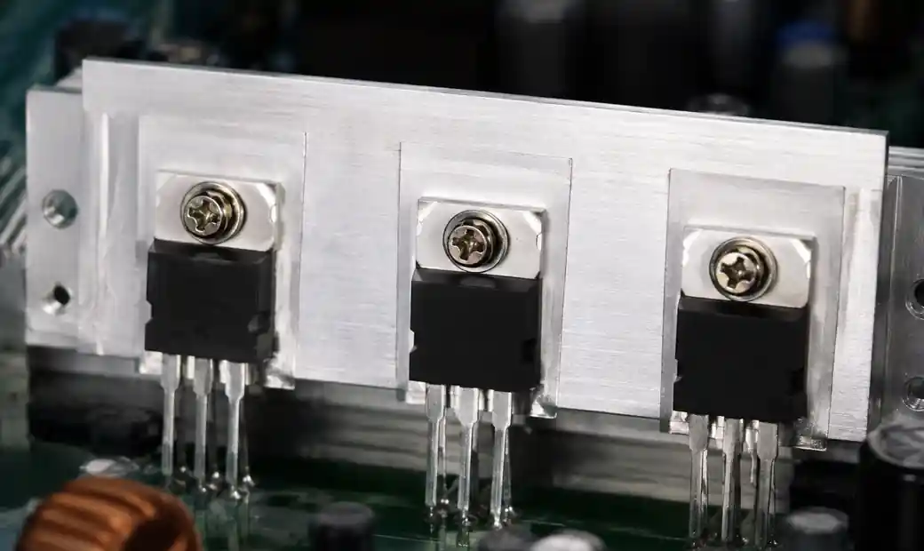 Multiple power MOSFETs mounted on common heat sink for thermal stability
Prevention Strategies
Emitter/Source Ballasting: Add 0.1-1Ω resistors in series with emitter/source for negative feedback. Essential for paralleling BJTs.
Temperature-Compensated Biasing: Use thermistor or diode in bias circuit to compensate VBE temperature coefficient in BJTs.
Thermal Coupling: Mount paralleled devices on common heat sink for temperature equalization.
Current Limiting: Incorporate current-sensing circuits that reduce drive or shut down when current exceeds thresholds.
Practical Design Examples
Example 1: Linear Regulator Thermal Design
12V to 5V linear regulator supplies 3A at TA(max) = 60°C.
Power Dissipation: PD = (12 - 5) × 3 = 21W
Specifications: θJC = 2°C/W (TO-220), TJ(design) = 125°C, θCS = 0.5°C/W
Required θSA: θSA = (125 - 60) / 21 - 2 - 0.5 = 0.6°C/W
Natural convection achieves 1-2°C/W for TO-220. Forced airflow (50-100 LFM) required.
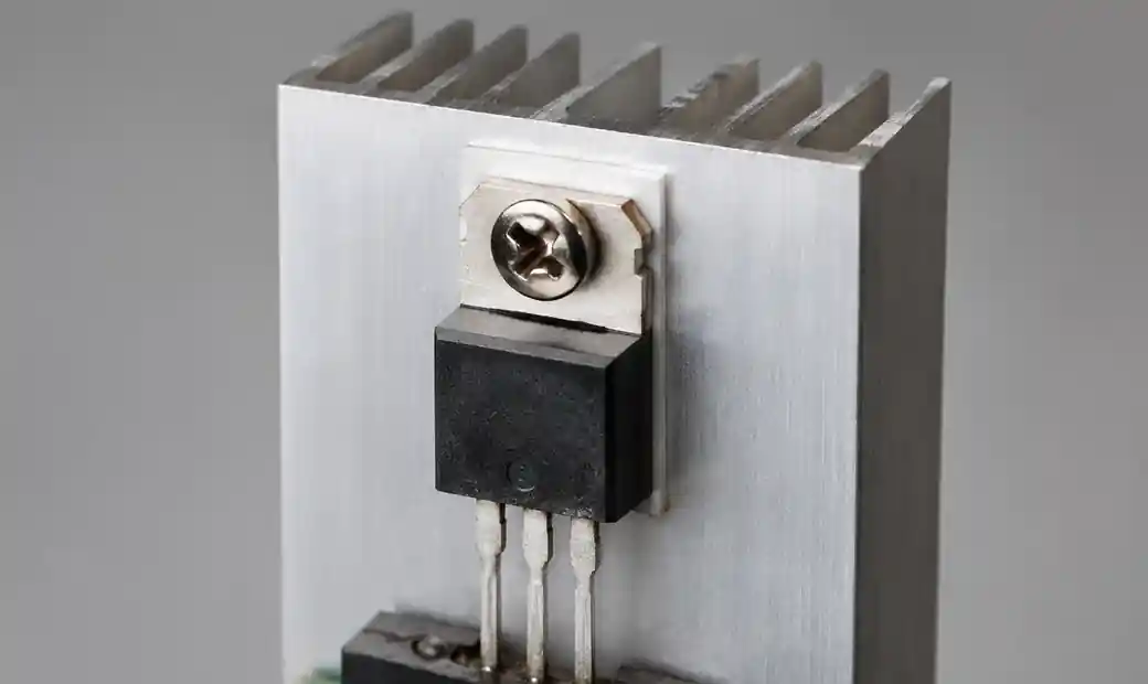 Linear voltage regulator with heat sink in TO-220 package assembly
Example 2: MOSFET Switching Application
600V, 20A MOSFET switches inductive load at 50 kHz, 50% duty cycle.
Conduction Loss: RDS(on) = 0.15Ω at 25°C, α = 0.005/°C At TJ = 125°C: RDS(on) = 0.15 × [1 + 0.005 × 100] = 0.225Ω PD(cond) = 20² × 0.225 × 0.5 = 45W
Switching Loss: VDS = 400V, tr + tf = 200ns PD(sw) = (400 × 20 × 200×10⁻⁹ × 50,000) / 2 = 40W
Total: PD = 85W
With θJC = 0.5°C/W, TA = 50°C, required θSA = (125 - 50) / 85 - 1.0 = -0.12°C/W
Solutions: reduce switching frequency, optimize gate drive, parallel MOSFETs, or use forced air.
Common Thermal Design Mistakes
Ignoring RDS(on) Temperature Coefficient: At 150°C, RDS(on) is 70-80% higher than 25°C values. Always apply temperature correction.
Insufficient Thermal Interface: Air gaps create 10°C/W resistance for TO-220. Thin uniform thermal grease layer is mandatory.
Operating at Maximum Ratings: Design for 125-135°C junction temperature, not 150-175°C maximum rating. Apply 20-30% margin.
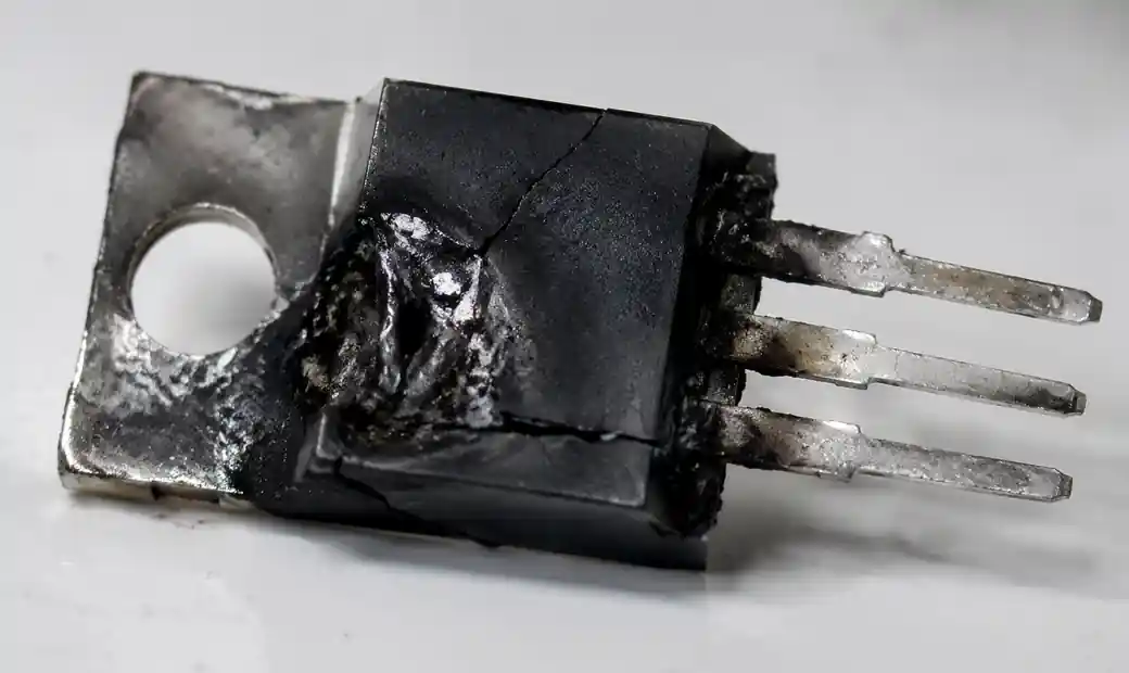 Failed power transistor showing thermal damage from inadequate heat sinking
Neglecting Switching Losses: Above 20 kHz, switching losses equal or exceed conduction losses. Gate drive design directly impacts losses.
Inadequate PCB Thermal Design: Surface-mount packages (D2PAK, DPAK) rely on copper area. Datasheets assume 1-2 square inches of 2oz copper.
FAQ
Q: What is the safe operating area (SOA) of a power transistor?
The SOA defines voltage and current boundaries for safe operation without damage. SOA curves plot voltage vs. current for different pulse durations, bounded by maximum current, voltage breakdown, power dissipation, and thermal limits. Always operate within temperature-derated SOA for your case temperature.
Q: How do I calculate junction temperature?
Use TJ = TA + (PD × θJA), where PD is total power dissipation and θJA is sum of junction-to-case, case-to-sink, and sink-to-ambient thermal resistances. Calculate PD including conduction losses (ID² × RDS(on)) and switching losses. Use RDS(on) corrected for operating temperature.
Q: What is the difference between θJC and θJA?
θJC (junction-to-case) is thermal resistance from die to package surface, specified in datasheets. θJA (junction-to-ambient) is total resistance from die to air, including package, thermal interface, heat sink, and convection. θJA varies with cooling; θJC is device constant.
Q: Why does RDS(on) increase with temperature?
Electron mobility in silicon decreases as temperature rises due to lattice vibration (phonon scattering). Temperature coefficient is +0.4% to +0.6% per °C. This positive coefficient provides thermal stability and enables safe paralleling of MOSFETs.
Q: How much thermal grease should I apply?
Apply thin uniform layer 0.05-0.1mm thick (50-75 microns)—barely visible. This fills microscopic air gaps while maintaining low thermal resistance. Excessive grease increases resistance instead of decreasing it.
Q: Can I parallel power transistors without current sharing resistors?
For MOSFETs, yes—positive temperature coefficient naturally balances current. For BJTs, no—emitter ballast resistors (0.1-1Ω) are mandatory because VBE decreases with temperature, causing current hogging. Always mount paralleled devices on common heat sink.
Q: What temperature should I design for in industrial applications?
Design for maximum junction temperature of 125-135°C even if rated to 150-175°C. This 20-30°C margin accounts for aging, thermal resistance degradation, and unexpected conditions, significantly improving MTTF. Ambient temperature typically 70-85°C for enclosed equipment, 50-60°C for ventilated.
Q: How do I reduce switching losses?
Use fast gate drivers with low impedance (1-5Ω gate resistance), MOSFETs with low gate charge (Qg), and optimal PCB layout with short gate traces. Select MOSFETs with low RDS(on) for your voltage rating. Consider soft-switching topologies (resonant converters, ZVS) for frequencies above 100 kHz.
Conclusion
Power transistor thermal design requires understanding SOA boundaries, accurate junction temperature calculation, and proper heat sink selection. SOA curves define operating limits that must be temperature-derated for actual conditions. Junction temperature calculations using thermal resistance models predict whether designs remain within safe limits, accounting for conduction and switching losses. Temperature derating by 15-25% extends operating lifetime significantly compared to maximum-rating operation.
If you need reliable power transistors and MOSFETs for industrial, automotive, or power conversion applications, Hitop Tech offers comprehensive procurement services with global sourcing across Asia, Europe, North America, and Africa. Our authorized distributor relationships ensure authentic components from leading semiconductor manufacturers. We provide technical support for component selection, thermal design verification, and supply chain optimization.
Contact us today for power transistor sourcing, thermal design consultation, and cost-effective supply chain solutions for your electronics projects.