



Isolated Gate Driver IC Selection for High Voltage Power Switches
Isolated gate driver IC selection for high-voltage power switches requires matching five critical parameters to your application: drive current capability (2-4A for IGBTs, 4-10A for SiC MOSFETs), isolation voltage rating (2.5-5kV industrial, 1.5kV automotive minimum), common-mode transient immunity above 100kV/μs for wide-bandgap devices, propagation delay matching within 5ns between channels, and integrated deadtime generation. Magnetic isolation has replaced optocouplers in high-performance designs due to superior CMTI ratings, stable timing across temperature, and elimination of LED aging drift.
Table of Contents
- Isolation Requirements
- Isolation Technology Comparison
- Drive Strength and Switching Speed
- Common-Mode Transient Immunity
- Propagation Delay and Timing
- Deadtime Control
- Half-Bridge vs Full-Bridge
- Application-Specific Criteria
- FAQ
- Conclusion
Isolation Requirements
Galvanic isolation protects control circuitry from high-voltage power stages while transmitting gate signals across the barrier. In applications above 400V, isolation prevents ground loops, blocks common-mode noise, and ensures safety during faults.
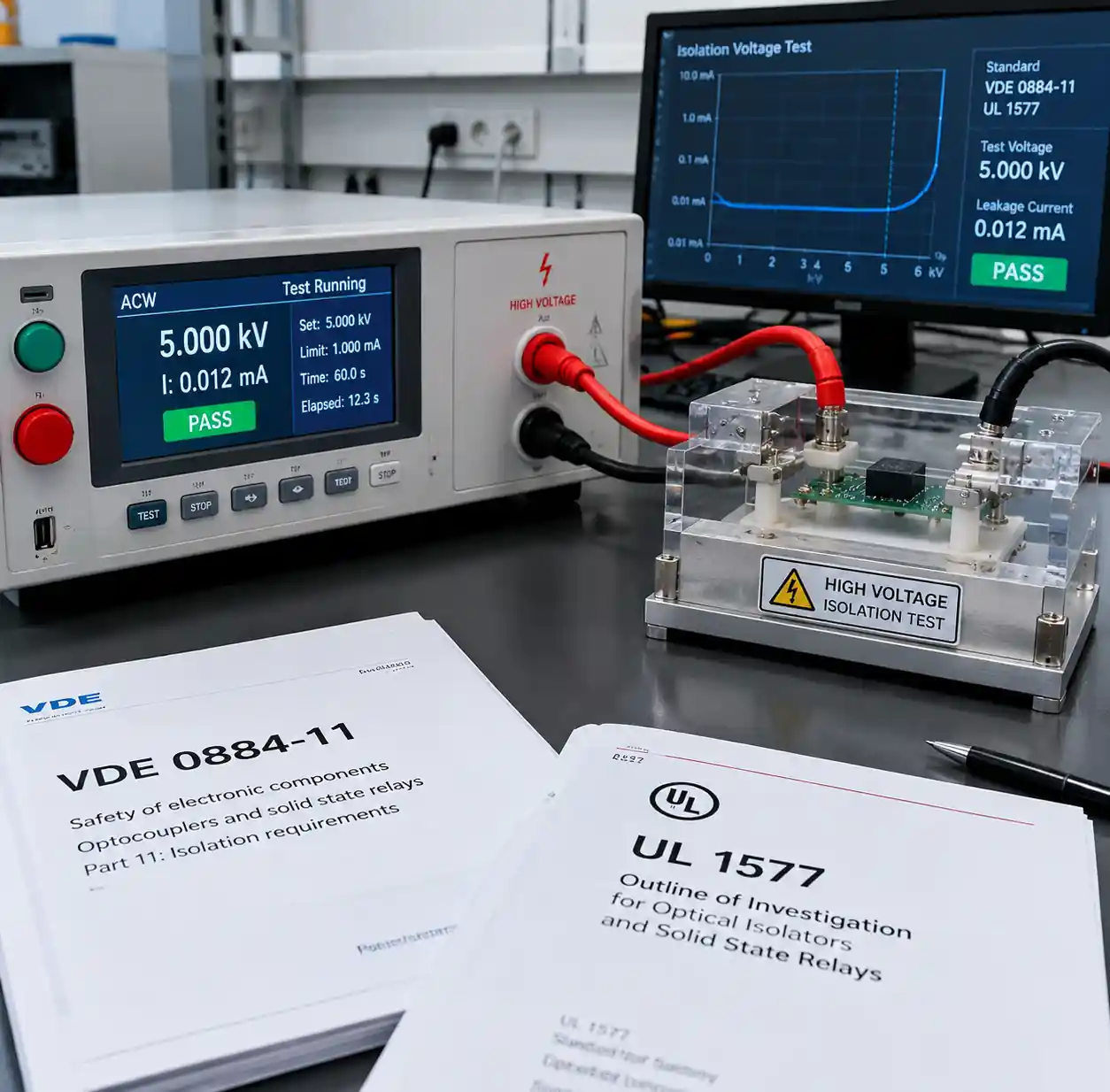 Industrial isolation voltage requirements for gate driver ICs showing VDE and UL standards compliance levels
Industrial systems require 2.5-5kV isolation per VDE 0884-11 or UL 1577 standards. Automotive traction inverters at 400-800V mandate 1.5kV minimum, with 2.5kV common for margin. Solar inverters need reinforced isolation—typically 5kV—for grid interconnection compliance.
Isolation voltage must exceed maximum working voltage with safety factor for transient overvoltages from lightning and switching surges. A 1200V SiC MOSFET half-bridge on 800V DC bus requires 2.5kV minimum isolation for 1.5× overvoltage capability.
Isolation Technology Comparison
Three isolation technologies serve gate driver applications: optocoupler, magnetic transformer, and capacitive. Performance differences determine which technology suits specific requirements.
| Isolation Type | CMTI | Propagation Delay | Timing Drift | Lifespan | Best Application |
|---|---|---|---|---|---|
| Optocoupler | 10-25 kV/μs | 50-200 ns | ±15-30% over life | LED aging limited | Legacy industrial <20kHz |
| Magnetic | 100-200 kV/μs | 25-50 ns | ±2-5% over temp | >25 years | SiC/GaN >100kHz, automotive |
| Capacitive | 50-100 kV/μs | 30-60 ns | ±3-8% over temp | >20 years | Mid-frequency IGBT, cost-sensitive |
Optocouplers use LED-photodetector pairs. LED aging causes propagation delay drift, complicating deadtime budgets. Avoid optocouplers above 20kHz or where CMTI exceeds 25kV/μs requirements.
Magnetic isolation uses on-die or packaged microtransformers, delivering highest CMTI for SiC and GaN devices generating 50V/ns+ dV/dt rates. Magnetic isolators maintain stable timing across temperature and operational life.
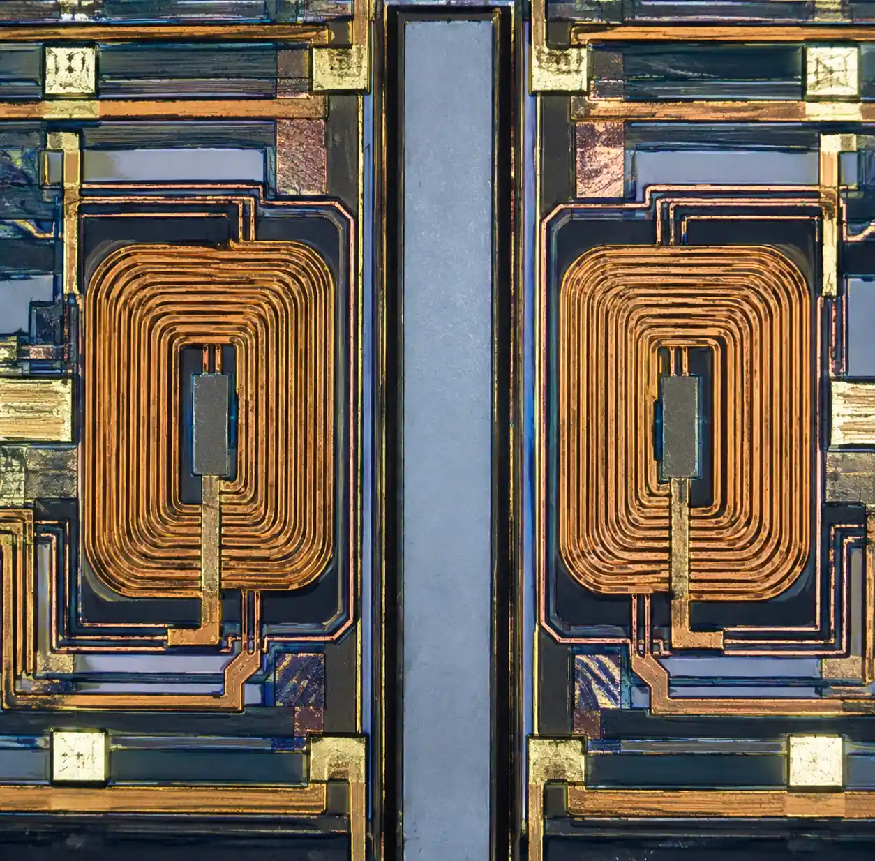 Magnetic isolation microtransformer structure inside gate driver IC package showing transformer coils
Capacitive isolation transmits signals through differential capacitor pairs across a dielectric barrier, balancing cost and performance for IGBT applications at 20-50kHz with CMTI below 75kV/μs.
Drive Strength and Switching Speed
Gate driver output current determines switching transition speed by charging and discharging power device gate capacitance. Insufficient drive strength extends switching time, increasing losses and risking linear-region failures.
IGBTs present 10-50nF gate charge. A 100A/1200V IGBT with 30nF capacitance needs 3A peak current for 10ns rise time (I = C × dV/dt with 10V swing). Modern IGBT drivers provide 2-4A peak capability.
SiC MOSFETs require higher drive currents for fast switching and negative gate voltage control. A 40A/1200V SiC MOSFET at 100kHz may need 5-10A peak current for 20ns transitions while controlling gate voltage during Miller plateau. Undersized drivers cannot overcome Miller capacitance feedback, extending switching times.
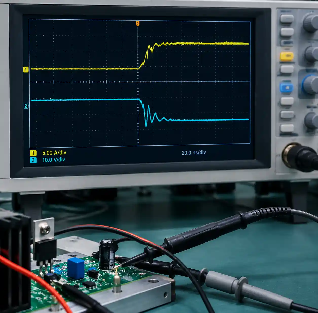 Oscilloscope measurement of gate driver peak output current charging MOSFET gate capacitance
Drivers must also sink current during turn-off, pulling gate voltage negative (typically -2V to -5V for SiC) to maintain off-state during high dV/dt transients. Asymmetric output stages with higher sink than source current enable fast turn-off for noise immunity.
Calculate required drive current: I_peak = Q_g / t_transition, where Q_g is datasheet gate charge and t_transition is target switching time. Add 50% margin for Miller plateau and parasitics.
For power semiconductor selection guidance, review our MOSFET vs IGBT guide.
Common-Mode Transient Immunity
CMTI quantifies a gate driver's ability to reject common-mode voltage transients without false output transitions. Specified in kV/μs, it represents maximum dV/dt the isolation barrier withstands while maintaining correct output state.
High-voltage converters generate severe common-mode transients during switching. A 1200V SiC MOSFET half-bridge switching 800V with 20ns rise time produces 40V/ns (40,000V/μs) dV/dt at the isolation barrier. If driver CMTI is only 25kV/μs—typical for optocouplers—this transient induces false triggering, causing shoot-through and device failure.
| Application | Typical dV/dt | Minimum CMTI | Driver Type |
|---|---|---|---|
| Si IGBT 600V (20kHz) | 5-10 V/ns | 25 kV/μs | Optocoupler or capacitive |
| Si IGBT 1200V (50kHz) | 15-25 V/ns | 50 kV/μs | Capacitive or magnetic |
| SiC MOSFET 1200V (100kHz) | 30-50 V/ns | 100 kV/μs | Magnetic isolation required |
| GaN FET 650V (500kHz) | 50-150 V/ns | 150 kV/μs | High-CMTI magnetic |
Modern magnetic isolation drivers achieve 100-200kV/μs CMTI through differential signaling and common-mode rejection. This specification determines whether drivers operate reliably in fast-switching wide-bandgap applications without excessive deadtime.
Insufficient CMTI forces increased deadtime—the period when both devices are off—to prevent false triggering. Excessive deadtime increases conduction losses and distorts PWM duty cycle, especially at high frequencies where deadtime becomes significant fraction of switching period.
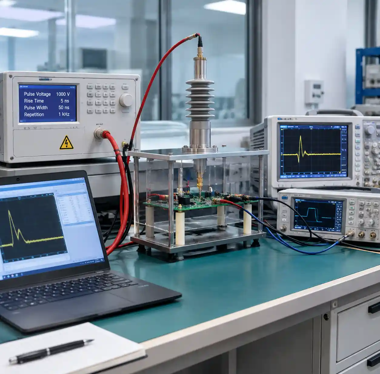 CMTI testing equipment measuring gate driver common-mode rejection during high dV/dt transients
High-CMTI drivers reduce required deadtime from 500-1000ns (optocouplers) to 100-200ns (magnetic isolation), improving converter efficiency by 1-3% at 100kHz switching frequency.
Propagation Delay and Timing
Propagation delay is time between input signal transition and output change. Absolute delay affects control loop bandwidth, while channel-to-channel matching prevents shoot-through in bridge configurations.
Modern isolated drivers exhibit 25-50ns propagation delays. At 100kHz switching with 25ns driver delay, phase shift is approximately 0.9°—acceptable for most control loops.
Channel-to-channel matching is critical. In half-bridge, if high-side driver has 30ns delay and low-side has 50ns, the 20ns mismatch must be absorbed in deadtime budget, increasing losses.
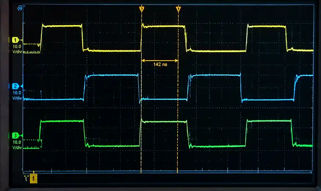 Dual-channel oscilloscope showing propagation delay timing mismatch between high-side and low-side gate drivers
Specify drivers with ±5ns maximum channel matching for half-bridge topologies. Premium drivers achieve ±2ns matching. Magnetic isolation exhibits ±5% delay variation from -40°C to +125°C, while optocouplers drift ±15-30% across same range.
Deadtime Control
Deadtime prevents shoot-through—simultaneous conduction of high-side and low-side devices creating DC bus short circuit. Gate drivers implement deadtime through internal logic, external RC networks, or microcontroller PWM.
Integrated deadtime generation eliminates external components and provides repeatable timing. Modern drivers include adjustable generators with resistor-programmed timing from 50ns to 2μs.
Calculate minimum deadtime: t_deadtime = t_prop_max - t_prop_min + t_fall + t_rise + t_margin, where propagation delay mismatch, device switching times, and safety margin (50-100ns) determine blanking interval.
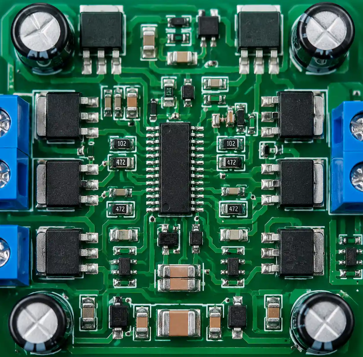 Gate driver PCB showing deadtime generation circuit with timing components and isolated channels
For SiC MOSFET half-bridge with 5ns driver delay matching, 15ns switching times, and 50ns margin, minimum deadtime is 85ns. Excessive deadtime beyond 150ns impacts efficiency through body diode conduction and duty cycle distortion.
Precision designs specify ±10% tolerance through integrated generators rather than external RC networks prone to component variation.
Half-Bridge vs Full-Bridge
Power converter topology determines gate driver requirements. Half-bridge controls one switching leg with high-side and low-side devices, while full-bridge uses four switches in two legs for bidirectional power flow.
Half-bridge gate drivers integrate two isolated channels with shared or independent inputs, bootstrap high-side supply, and deadtime generation in single package. Applications include DC-DC converters, motor inverters, and PFC stages.
Bootstrap supply circuits power high-side driver by charging capacitor during low-side on-time. Bootstrap operation requires minimum 5-10% duty cycle to refresh capacitor. Applications with extended high-side on-times (>95% duty) need isolated auxiliary supplies.
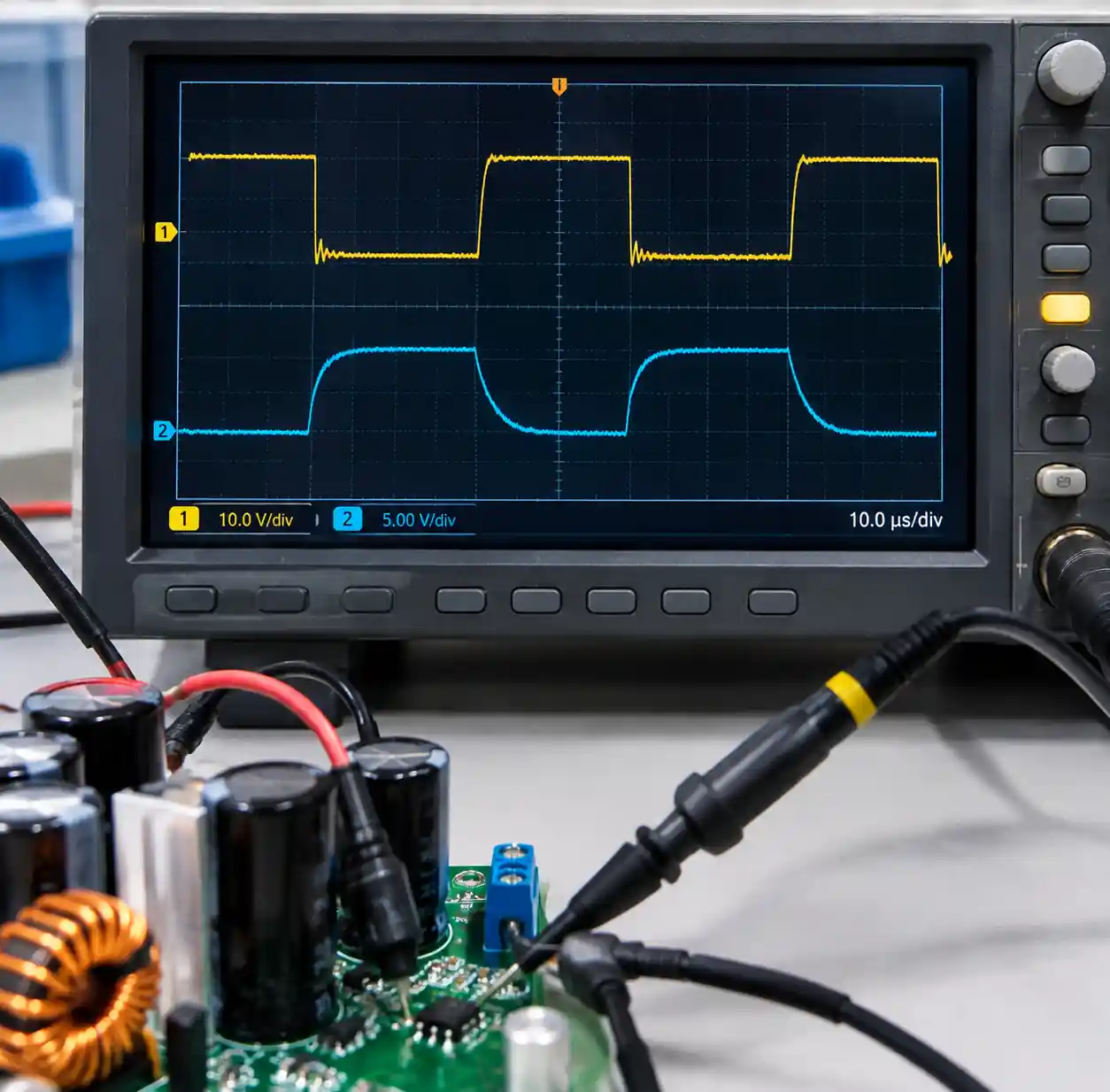 Bootstrap capacitor voltage waveform in half-bridge gate driver during high-side switching operation
Full-bridge configurations demand channel synchronization to prevent cross-conduction. Specify drivers with matched propagation delays across all four channels. Some full-bridge drivers include interlocking logic preventing simultaneous enable signals to opposing devices.
For electronic component procurement and product lifecycle management support, Hitop Tech Limited provides sourcing solutions for gate driver ICs and power semiconductors.
Application-Specific Criteria
Different applications impose distinct requirements beyond core gate driver specifications.
Automotive traction inverters require AEC-Q100 qualification, -40°C to +150°C junction temperature, and built-in diagnostics for ISO 26262 functional safety. These systems operate at 10-20kHz with SiC MOSFETs, requiring 100kV/μs CMTI and ±2A drive current.
Industrial motor drives from 1-500kW prioritize cost-effectiveness and robustness. IGBT-based designs at 4-16kHz can use capacitive or magnetic isolation with 50kV/μs CMTI and ±2A drive current. Built-in desaturation detection prevents shoot-through during faults.
Solar inverters and energy storage systems demand high efficiency across wide load ranges. Applications use silicon or SiC IGBTs at 20-50kHz, requiring magnetic isolation with 75-100kV/μs CMTI and reinforced isolation for grid compliance.
Telecommunications power supplies and server PSUs prioritize density and efficiency. LLC resonant converters use integrated half-bridge drivers with adaptive deadtime, achieving >95% efficiency at 100-500kHz. GaN FET compatibility requires 150kV/μs CMTI and 5A peak drive current.
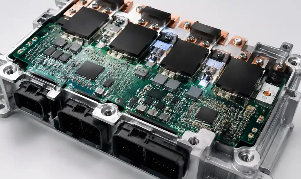 Automotive-grade isolated gate driver module for SiC MOSFET traction inverter showing power electronics assembly
Explore our electronic components categories and application case studies for selection guidance.
FAQ
What is the minimum CMTI rating for SiC MOSFET gate drivers?
SiC MOSFETs switching 1200V at 100kHz generate 30-50V/ns dV/dt rates, requiring minimum 100kV/μs CMTI. Specify 150kV/μs for 650V GaN FETs above 500kHz. Lower CMTI causes false triggering and excessive deadtime.
Can I use optocoupler-based drivers for wide-bandgap devices?
No. Optocouplers offer only 10-25kV/μs CMTI, insufficient for the 50-150V/ns dV/dt rates SiC and GaN generate. LED aging causes timing drift. Use magnetic isolation for wide-bandgap semiconductors.
How do I calculate required gate driver output current?
Use I_peak = Q_g / t_transition where Q_g is gate charge from datasheet and t_transition is target switching time. Add 50% margin for Miller plateau. A 30nC device switched in 15ns requires minimum 2A peak, so specify 3A driver.
What propagation delay matching is required for half-bridge drivers?
Specify ±5ns maximum channel-to-channel mismatch for reliable operation. Premium drivers achieve ±2ns matching. Larger mismatches increase deadtime losses. Verify matching across full temperature range (-40°C to +125°C).
Do I need integrated deadtime generation or external timing?
Integrated deadtime generation reduces component count and provides better accuracy. Modern drivers offer resistor-programmable timing from 50ns to 2μs with ±10% tolerance. External RC timing drifts ±20-30% across temperature.
What bootstrap capacitor value is required for half-bridge drivers?
Calculate C_boot = 20 × Q_g + I_leak / f_sw where Q_g is gate charge, I_leak is quiescent current, and f_sw is switching frequency. Typical values range 0.1-4.7μF. Applications with >95% duty cycle require isolated auxiliary supplies.
Conclusion
Isolated gate driver selection balances drive current capability, isolation voltage rating, CMTI performance, propagation delay matching, and deadtime control against application requirements. Modern magnetic isolation has superseded optocouplers in high-performance applications through superior CMTI above 100kV/μs, stable timing, and immunity to aging.
For SiC and GaN applications, specify minimum 100-150kV/μs CMTI, 4-10A peak drive current, and ±5ns delay matching. IGBT applications at moderate frequencies can use capacitive isolation with 50-75kV/μs CMTI and ±2A drive current. Integrated deadtime generation simplifies design versus external timing networks.
As switching frequencies increase and wide-bandgap adoption accelerates, high-CMTI magnetic isolation becomes essential for reliable power conversion. For technical support in gate driver and power semiconductor selection, contact Hitop Tech Limited or submit requirements through our RFQ system.