


NAND vs NOR Flash Memory: A Technical Selection Guide for Embedded Systems
Table of Contents
- Introduction: Why Flash Memory Architecture Matters
- Key Technical Parameters Explained
- Architecture Differences and Their Engineering Impact
- Performance Comparison: Read, Write, and Erase Operations
- Application-Specific Selection Criteria
- Design Considerations and Common Pitfalls
- Supply Chain and Sourcing Considerations
- FAQ
1. Introduction: Why Flash Memory Architecture Matters
Choosing between NAND and NOR flash memory is one of the most critical decisions in embedded system design. These two flash architectures are fundamentally different in their physical structure, performance characteristics, and optimal use cases. Making the wrong choice can result in inadequate performance, increased costs, or even complete system redesign.
NAND and NOR flash memory are both non-volatile storage technologies based on floating-gate transistor cells. However, their memory cell arrangements—resembling their respective logic gate configurations—create distinct trade-offs in speed, density, cost, and reliability. For engineers working on automotive, industrial, IoT, or consumer electronics projects, understanding these differences is essential for optimal component selection.
This guide provides a technical comparison of NAND vs NOR flash memory, focusing on the parameters that matter most for design decisions: read/write performance, storage density, execute-in-place capability, endurance, and total cost of ownership. Whether you're selecting flash for firmware storage, data logging, or mass storage applications, this article will help you make an informed choice based on your specific requirements.
Target readers: This guide is written for PCB design engineers, embedded systems developers, hardware architects, and procurement managers who need to understand the technical trade-offs between NAND and NOR flash memory for component selection and system design.
2. Key Technical Parameters Explained
When comparing NAND and NOR flash memory, several technical parameters directly influence performance, reliability, and suitability for specific applications. Understanding these parameters is crucial for making informed selection decisions.
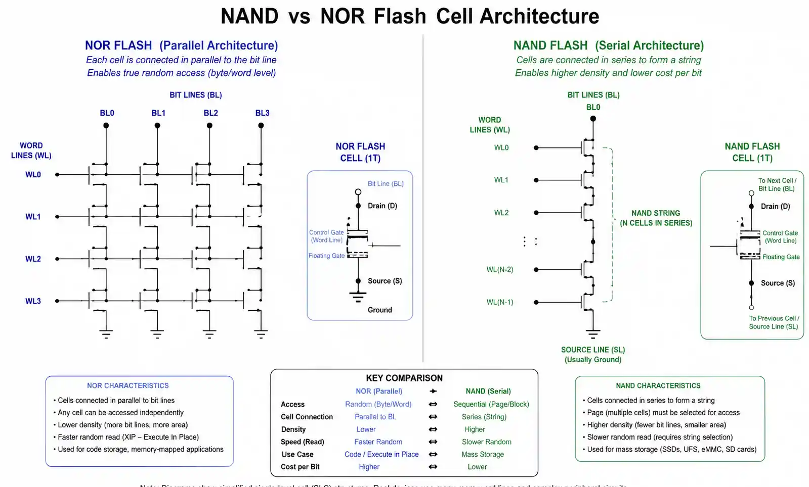
2.1 Cell Architecture and Logic Gate Analogy
NOR Flash Architecture: In NOR flash, each memory cell is connected in parallel between the bit line and ground, with one transistor per bit. This configuration resembles a NOR logic gate, where any cell can be accessed independently. The parallel structure enables true random access at the byte level, allowing the processor to execute code directly from the memory (execute-in-place or XIP).
NAND Flash Architecture: NAND flash connects multiple memory cells (typically 8 to 32) in series to form a string, similar to a NAND logic gate configuration. This series connection reduces the number of contacts needed per cell, dramatically increasing storage density. However, it requires block-level addressing rather than byte-level access.
2.2 Access Granularity and Addressing
NOR flash supports byte-level random access with typical addressing down to 8-bit or 16-bit words. This makes it ideal for code storage where random instruction fetches are common.
NAND flash uses page-based addressing, with typical page sizes of 2KB, 4KB, or 8KB. Data must be read or written in entire pages, and erase operations occur at the block level (typically 128KB to 512KB blocks). This structure optimizes sequential data access but introduces latency for random reads.
2.3 Endurance and Write Cycles
Flash memory cells degrade with each program-erase (P/E) cycle due to charge trapping in the oxide layer. Endurance varies significantly between architectures and cell types:
- NOR flash: Typically 10,000 to 100,000 P/E cycles for standard NOR, with some industrial-grade parts rated up to 1 million cycles
- SLC NAND: 50,000 to 100,000 P/E cycles
- MLC NAND: 3,000 to 10,000 P/E cycles
- TLC NAND: 500 to 3,000 P/E cycles
For applications requiring frequent updates (like data logging or wear-intensive workloads), SLC NAND or NOR flash typically provides better endurance than MLC or TLC NAND.
2.4 Error Correction Requirements
NAND flash is inherently more prone to bit errors due to its high-density cell structure and charge leakage over time. Error correction code (ECC) is mandatory for NAND flash, with requirements ranging from 1-bit ECC per 512 bytes for SLC NAND to 40-bit or higher ECC per 1KB for TLC NAND.
NOR flash has significantly lower bit error rates and can often operate without ECC in many applications, though industrial and automotive designs typically implement ECC for additional data integrity.
3. Architecture Differences and Their Engineering Impact
The fundamental architectural differences between NAND and NOR flash create cascading effects throughout the design process. Understanding these impacts helps engineers avoid costly mistakes during component selection and PCB layout.
3.1 Memory Cell Structure
In NOR flash, each cell connects directly to a bit line and source line, forming a parallel array. This parallel structure requires more silicon area per bit, resulting in lower storage density but enabling true random access. The direct connection to bit lines allows for fast read operations with minimal latency.
In NAND flash, cells are organized in series strings, with only the string endpoints connecting to bit lines. This serial configuration dramatically reduces the number of contacts and increases density, but introduces read latency because the entire string must be activated to access a single cell.
3.2 Execute-in-Place (XIP) Capability
NOR flash supports XIP, meaning the processor can execute code directly from the flash memory without first copying it to RAM. This capability is critical for:
- Boot code and firmware storage
- Resource-constrained systems with limited RAM
- Real-time systems requiring deterministic code execution
- Applications where code updates are infrequent
NAND flash does not support XIP due to its page-based access structure. Code stored in NAND must first be copied to RAM for execution, requiring:
- Additional RAM capacity for shadowing
- Boot loader complexity to manage code transfer
- Increased boot time
- File system or flash translation layer (FTL) for wear leveling and bad block management
| Parameter | NOR Flash | NAND Flash |
|---|---|---|
| XIP Support | Yes - Direct code execution | No - Must copy to RAM |
| Boot Time | Fast (1-10ms typical) | Slower (10-100ms typical) |
| RAM Requirements | Minimal | Significant (code shadow) |
| Boot Loader Complexity | Simple | Complex (FTL required) |
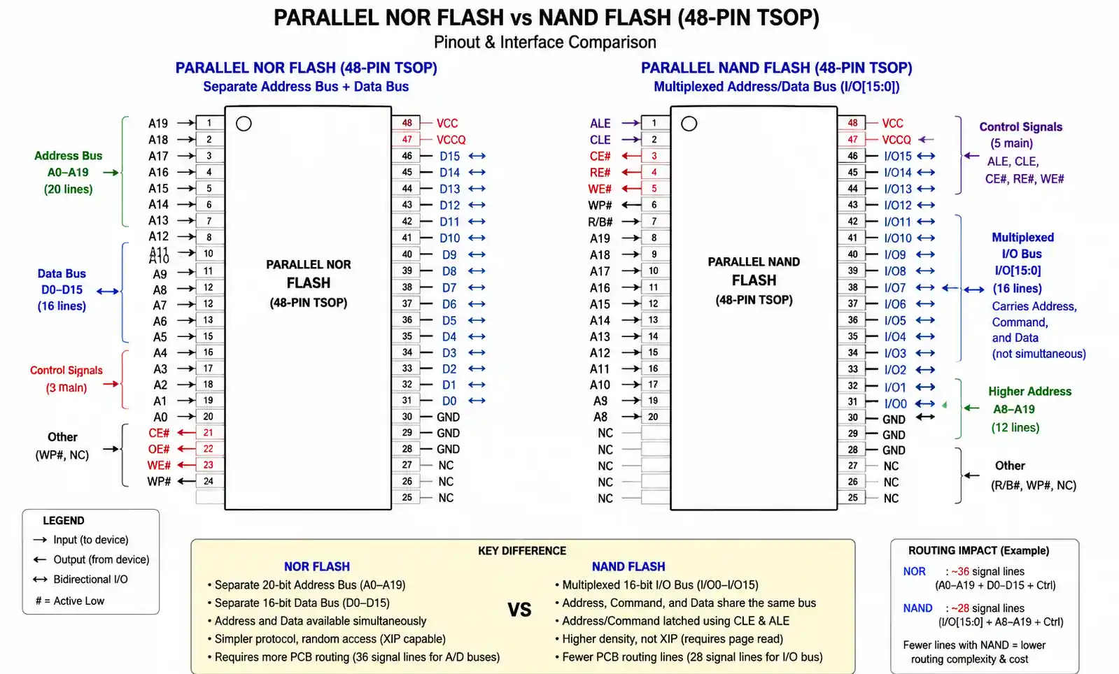
3.3 Interface and Pin Count
NOR flash typically uses a parallel interface with separate address and data buses, resulting in pin counts of 32 to 56 pins for parallel NOR. Serial NOR (SPI or Quad SPI) reduces this to 6-10 pins but at lower bandwidth.
NAND flash commonly uses an 8-bit or 16-bit multiplexed bus with fewer control signals, resulting in lower pin counts (typically 16-48 pins). Modern NAND also offers serial interfaces like SPI NAND and e.MMC/UFS for further pin reduction.
For space-constrained designs or cost-sensitive applications, the lower pin count of NAND flash can simplify PCB routing and reduce package costs.
4. Performance Comparison: Read, Write, and Erase Operations
Performance characteristics differ dramatically between NAND and NOR flash across read, write, and erase operations. These differences directly influence system responsiveness, throughput, and power consumption.
4.1 Read Performance
NOR flash excels in random read operations with typical access times of 25ns to 150ns for parallel NOR. Sequential read throughput ranges from 50 MB/s to 100 MB/s for parallel NOR and 20 MB/s to 80 MB/s for Quad SPI NOR.
NAND flash has higher latency for initial page access (typically 10µs to 50µs) but delivers superior sequential throughput once the page is loaded. Sequential read speeds range from 40 MB/s for basic SPI NAND to over 500 MB/s for modern e.MMC 5.1 or UFS 3.1 NAND.
| Flash Type | Random Read Latency | Sequential Read Speed | Best Use Case |
|---|---|---|---|
| Parallel NOR | 25-150ns | 50-100 MB/s | Code execution, frequent random access |
| SPI NOR (Quad) | 0.5-2µs | 20-80 MB/s | Firmware storage, boot code |
| SLC NAND | 10-25µs | 40-200 MB/s | Data storage, sequential access |
| MLC NAND | 25-50µs | 100-400 MB/s | Mass storage, high throughput |
| e.MMC 5.1 | 15-30µs | 250-400 MB/s | Embedded storage, multimedia |
4.2 Write Performance
NOR flash write operations are significantly slower than reads, with typical page program times of 100µs to 1ms per byte or page. Write throughput generally ranges from 10 KB/s to 500 KB/s, making NOR unsuitable for write-intensive applications.
NAND flash offers much faster write performance with page program times of 200µs to 1ms per 2KB-8KB page. Sequential write throughput ranges from 10 MB/s for basic NAND to over 200 MB/s for modern e.MMC or UFS NAND.
4.3 Erase Operations
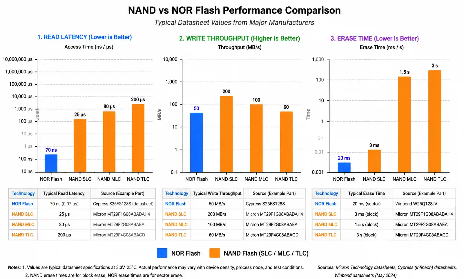
Both NAND and NOR flash require erase operations before programming, but their erase characteristics differ significantly:
NOR flash erase times are substantially longer, with sector erase (typically 64KB to 256KB) taking 0.5s to 3s per sector. Full chip erase can take 30s to several minutes.
NAND flash erase operations are faster, with block erase (typically 128KB to 512KB) completing in 2ms to 10ms per block.
| Operation | NOR Flash | NAND Flash | Impact |
|---|---|---|---|
| Erase Granularity | 64-256KB sectors | 128-512KB blocks | NAND requires careful wear leveling |
| Erase Time | 0.5-3s per sector | 2-10ms per block | NOR erase is 100-300x slower |
| Write-After-Erase | Required | Required | Both require FTL or wear leveling |
The slow erase performance of NOR flash makes it unsuitable for applications requiring frequent large-scale data updates, such as data logging or file storage systems.
5. Application-Specific Selection Criteria
Selecting between NAND and NOR flash depends heavily on the specific requirements of your application. This section provides decision frameworks for common embedded system scenarios.
5.1 Firmware and Boot Code Storage
Recommended: NOR Flash
For applications where firmware is stored and executed directly, NOR flash is typically the optimal choice due to:
- Execute-in-place (XIP) capability eliminates RAM shadowing requirements
- Fast random read access ensures responsive code execution
- Simple boot architecture without FTL complexity
- Lower bit error rates reduce ECC overhead
- Byte-level writes enable efficient firmware updates
Typical applications: MCU boot code, BIOS/UEFI firmware, communication protocol stacks, real-time operating systems (RTOS), automotive ECU firmware.
5.2 Mass Data Storage
Recommended: NAND Flash
For applications requiring large amounts of non-volatile storage (>128MB), NAND flash provides:
- 5-10x higher storage density than NOR
- Significantly lower cost per gigabyte ($0.10-0.50/GB for NAND vs $2-10/GB for NOR)
- Faster sequential write performance for data logging
- Established file systems (FAT, ext4, F2FS) optimized for NAND
Typical applications: Industrial data loggers, automotive event recorders, multimedia storage, IoT edge devices, portable instruments.
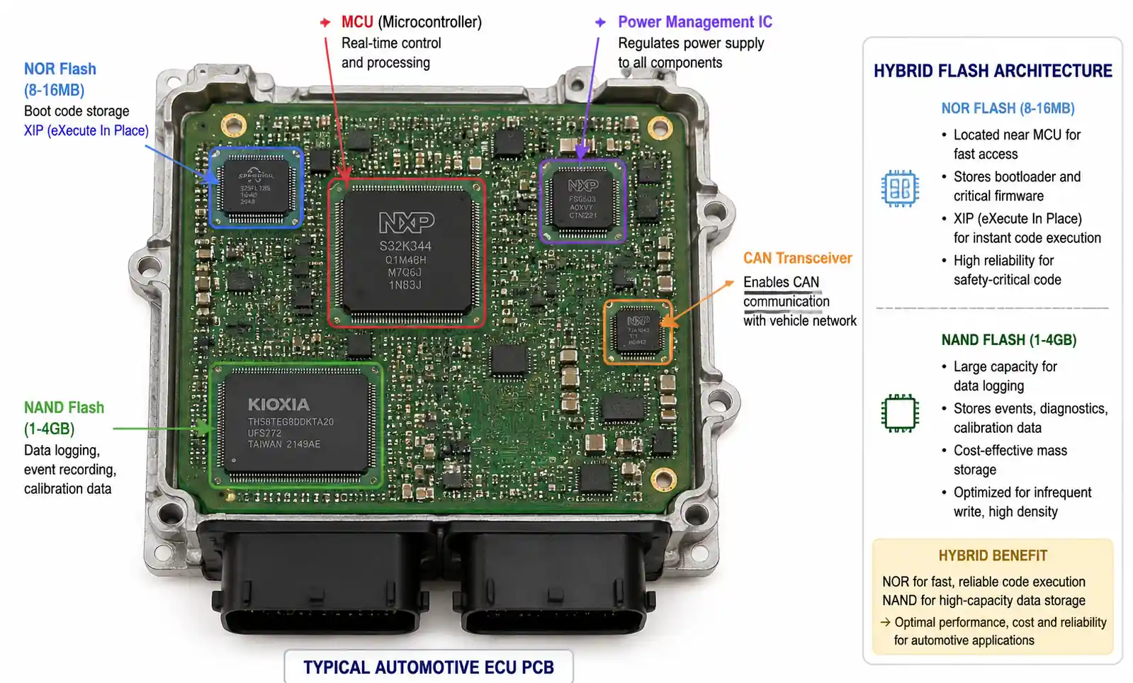
5.3 Mixed-Use Systems
Recommended: NOR + NAND Hybrid
Many systems benefit from using both flash types:
- Small NOR flash (4-32MB) for boot code and critical firmware
- Larger NAND flash (1GB+) for data storage and user files
- Separates code execution from data storage for optimal performance
Typical applications: Industrial HMIs, automotive infotainment, medical devices, network equipment, advanced IoT gateways.
5.4 Automotive and Industrial Environments
For harsh environment applications (AEC-Q100, industrial temperature -40°C to +85°C), additional considerations apply:
| Selection Factor | NOR Flash Advantage | NAND Flash Advantage |
|---|---|---|
| Temperature Stability | Better data retention at high temps | Requires temperature-compensated ECC |
| Safety-Critical Code | XIP simplifies functional safety | Not suitable for direct code execution |
| Data Logging | Slow writes limit throughput | High write throughput and capacity |
| Endurance | Good for frequent small updates | SLC NAND matches or exceeds NOR |
| Supply Chain | Longer product lifecycles (10+ years) | Faster technology transitions |
For automotive applications requiring ASIL-B or higher functional safety ratings, NOR flash is often preferred for code storage due to its deterministic access patterns and XIP capability.
6. Design Considerations and Common Pitfalls
Experienced embedded systems engineers know that flash memory selection extends beyond the datasheet parameters. This section covers critical design considerations and mistakes to avoid.
6.1 Error Correction and Data Integrity
Critical mistake: Underestimating ECC requirements for NAND flash.
NAND flash requires robust ECC to maintain data integrity over its lifetime. As NAND cells wear through program-erase cycles, bit error rates increase. The required ECC strength depends on the NAND type:
- SLC NAND: 1-4 bit ECC per 512 bytes minimum
- MLC NAND: 4-24 bit ECC per 1KB
- TLC NAND: 40-80 bit ECC per 1KB or higher
Insufficient ECC leads to uncorrectable errors and data corruption as the device ages. Always implement ECC that exceeds the manufacturer's minimum specification, especially for industrial temperature ranges and long product lifetimes.
NOR flash has inherently lower bit error rates (typically 10^-17 to 10^-15 bit error rate) but should still implement ECC for automotive and industrial applications to ensure data integrity over temperature extremes and radiation exposure.
6.2 Wear Leveling and Endurance Management
Critical mistake: Ignoring wear leveling requirements for NAND flash.
NAND flash requires wear leveling algorithms to distribute write and erase cycles evenly across all blocks. Without proper wear leveling:
- Frequently written blocks wear out prematurely
- Bad blocks accumulate faster than expected
- Device lifetime is dramatically reduced
Implement wear leveling through:
- Hardware controllers: e.MMC, managed NAND with built-in FTL
- Software FTL: JFFS2, UBIFS, or proprietary flash file systems
- Middleware: FatFs with wear leveling layer, littlefs
For NOR flash, wear leveling is less critical but still recommended for applications with frequent updates to specific sectors (e.g., configuration data, calibration values).
6.3 Over-Provisioning for Longevity
Best practice: Reserve 10-20% of NAND flash capacity for over-provisioning.
Over-provisioning provides spare blocks for wear leveling and bad block replacement, extending device lifetime. For a 1GB NAND flash, allocate only 800-900MB to the file system, reserving the remainder for the FTL.
6.4 Power Loss Protection
Critical mistake: Inadequate power fail handling for NAND writes.
NAND flash page program operations take 200µs to 1ms. If power fails during programming, the page may be corrupted or partially written. Implement power fail protection through:
- Capacitor holdup circuits providing 5-10ms of backup power
- Atomic write operations with transaction logging
- File systems designed for power-fail resilience (F2FS, littlefs)
NOR flash is more resilient to power failures during write operations but still benefits from proper power fail handling for mission-critical data.
6.5 Temperature Effects on Retention
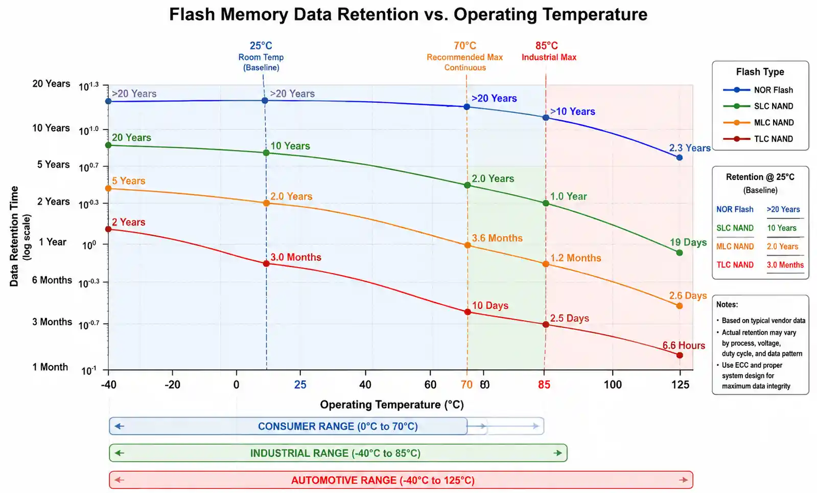
Flash memory data retention decreases exponentially with temperature. At 85°C, NAND flash retention may drop to 1 year or less, compared to 10+ years at 25°C. For industrial and automotive applications:
- Use SLC NAND for better retention at high temperatures
- Implement periodic data scrubbing (read-verify-rewrite)
- Design thermal management to keep flash temperature below 70°C during operation
- Consider industrial-grade NOR flash for critical code storage in high-temperature environments
| Flash Type | Retention at 25°C | Retention at 85°C | Recommended Action |
|---|---|---|---|
| NOR Flash | 20+ years | 10+ years | Suitable for high-temp code storage |
| SLC NAND | 10 years | 1-2 years | Implement data scrubbing every 3-6 months |
| MLC NAND | 5-10 years | 6-12 months | Limit to moderate-temp applications |
| TLC NAND | 1-3 years | 3-6 months | Not recommended for industrial temps |
7. Supply Chain and Sourcing Considerations
Beyond technical parameters, supply chain factors significantly impact flash memory selection for production designs.
7.1 Cost Comparison
NAND flash offers dramatically lower cost per gigabyte, making it economical for storage capacities above 512MB:
- NAND flash: $0.10-0.50 per GB (depending on type and volume)
- NOR flash: $2-10 per GB
However, for small capacities (<64MB), NOR flash may be cost-competitive when considering:
- No need for external DRAM for code shadowing
- Simpler system architecture without FTL
- Reduced software development and testing costs
7.2 Product Lifecycle and Obsolescence
NOR flash typically has longer product lifecycles (10-15 years) with better availability for legacy designs. Major NOR manufacturers include Micron, Cypress (Infineon), Winbond, and Macronix, many offering automotive-grade and industrial-grade parts with extended production commitments.
NAND flash technology evolves rapidly with frequent transitions to smaller process nodes and higher bit densities. This creates obsolescence risks for long-lifecycle products. Consider:
- e.MMC or managed NAND solutions that abstract underlying NAND changes
- Second-sourcing strategies with pin-compatible alternatives
- Working with distributors offering product change notifications
7.3 Lead Times and MOQ
During supply chain disruptions (such as 2020-2022), flash memory lead times stretched from 12-16 weeks to over 52 weeks. Current lead times (as of 2026) have normalized to 8-16 weeks for most standard parts.
Strategies to mitigate supply risk:
- Qualify multiple suppliers during design phase
- Use industry-standard packages (SOIC-8, WSON, BGA) with multiple sources
- Consider e.MMC or UFS for NAND to enable vendor flexibility
- Maintain safety stock for products in mass production
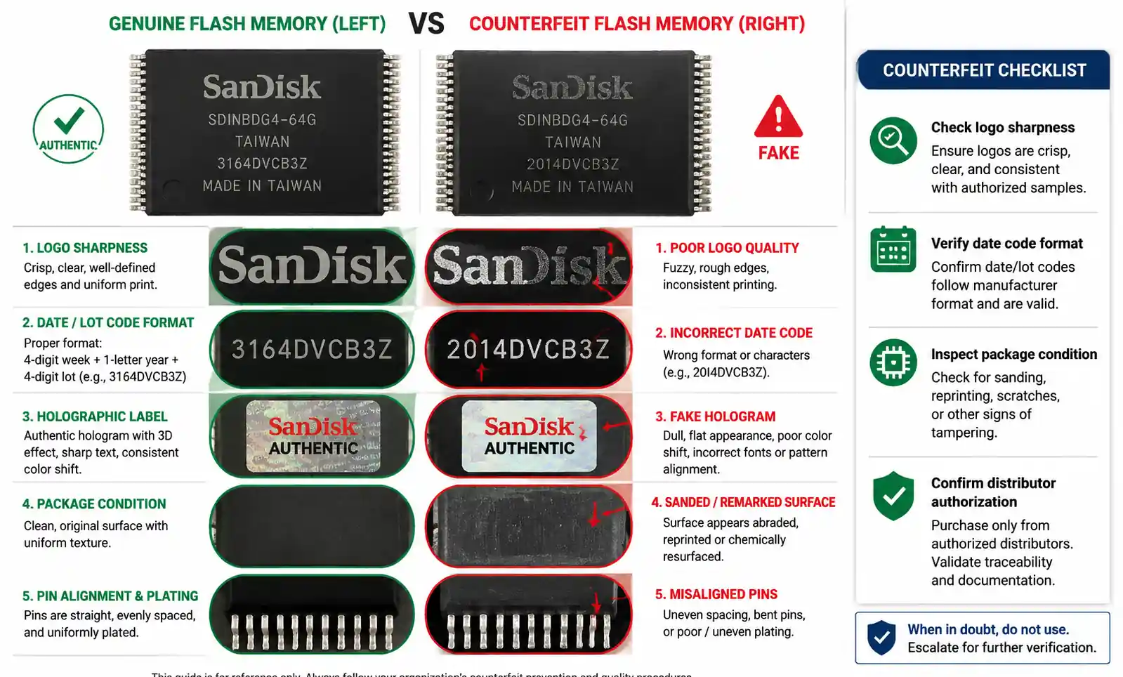
7.4 Counterfeit Risk and Authorized Distribution
Flash memory is a common target for counterfeiters. Always source from authorized distributors such as Digi-Key, Mouser, Avnet, or Arrow. For high-volume production, establish direct relationships with manufacturers.
Red flags for counterfeit flash:
- Pricing significantly below market rates
- Missing or incorrect lot codes and date codes
- Performance inconsistencies across batches
- Premature failures in field testing
8. FAQ
Q1: Can I replace NOR flash with NAND flash in an existing design?
No, not without significant design changes. NAND flash does not support execute-in-place (XIP), so code cannot run directly from NAND. You would need to add sufficient RAM to shadow code from NAND, implement a flash translation layer (FTL) for wear leveling and bad block management, and redesign your boot architecture. The system software would require substantial modifications to support NAND's page-based access model rather than NOR's byte-level access.
Q2: What does SLC, MLC, and TLC mean, and which should I choose?
SLC (Single-Level Cell) stores 1 bit per cell, MLC (Multi-Level Cell) stores 2 bits per cell, and TLC (Triple-Level Cell) stores 3 bits per cell. SLC offers the best endurance (50,000-100,000 P/E cycles), fastest write speeds, and lowest bit error rates, but costs 2-3x more than MLC and 4-6x more than TLC. For industrial and automotive applications, SLC NAND is strongly recommended. For consumer applications with shorter lifetimes, MLC or TLC may be acceptable with proper ECC and wear leveling.
Q3: How do I calculate the actual usable lifetime of NAND flash?
Calculate lifetime using the formula: Lifetime (years) = (Total blocks × P/E cycles × Block size) / (Daily write volume × 365 × Write amplification factor). For example, a 4GB SLC NAND with 100,000 P/E cycles, 128KB blocks, writing 100MB daily with 2x write amplification: (32,768 blocks × 100,000 × 128KB) / (100MB × 365 × 2) ≈ 57 years. Always include 10-20% over-provisioning and account for temperature effects on endurance.
Q4: Is ECC required for NOR flash?
For consumer and commercial applications, NOR flash can often operate reliably without ECC due to its low intrinsic bit error rate. However, for automotive (AEC-Q100), industrial, or safety-critical applications, implementing ECC is strongly recommended to ensure data integrity over temperature extremes, voltage variations, and radiation exposure. Even simple 1-bit or 2-bit ECC per word significantly improves reliability.
Q5: What is the difference between raw NAND and managed NAND (e.MMC)?
Raw NAND requires the host processor to implement all flash management functions including error correction, wear leveling, bad block management, and garbage collection. Managed NAND solutions like e.MMC, UFS, or SSD controllers integrate these functions in hardware, presenting a simple block-device interface to the host. Managed NAND simplifies software development and enables vendor migration but costs 20-50% more than raw NAND. For complex systems or teams without deep flash expertise, managed NAND significantly reduces development risk.
Q6: Can I use NAND flash for automotive applications?
Yes, but with careful consideration. SLC NAND is preferred for automotive applications due to its superior endurance, lower bit error rates, and better temperature performance compared to MLC or TLC. Many automotive-qualified NAND flash parts are available with AEC-Q100 certification. For safety-critical code storage (ASIL-B or higher), NOR flash is typically preferred due to its XIP capability and deterministic access patterns. A hybrid approach using NOR for code and NAND for data storage is common in automotive systems.
Q7: How does temperature affect flash memory reliability?
Temperature dramatically impacts both data retention and endurance. At 85°C, NAND flash retention drops from 10 years (at 25°C) to 1 year or less. Each 10°C increase in operating temperature roughly halves data retention time. Additionally, high temperatures accelerate cell wear, reducing effective P/E cycle endurance. For industrial applications operating at elevated temperatures, implement data scrubbing (periodic read-verify-rewrite), use SLC NAND or industrial-grade NOR, and design thermal management to minimize flash die temperature.
Q8: What is execute-in-place (XIP) and why does it matter?
Execute-in-place (XIP) allows the processor to fetch and execute instructions directly from flash memory without first copying them to RAM. This capability, unique to NOR flash, reduces RAM requirements, simplifies boot architecture, and enables deterministic real-time code execution. For resource-constrained MCU-based systems or safety-critical applications requiring predictable timing, XIP is often essential. NAND flash does not support XIP due to its page-based access structure, requiring code to be loaded into RAM before execution.
Conclusion
Choosing between NAND and NOR flash memory requires careful analysis of your application's specific requirements across performance, capacity, cost, and reliability dimensions. The decision framework is straightforward:
Choose NOR flash when:
- You need execute-in-place (XIP) capability for direct code execution
- Random read performance and low latency are critical
- Storage capacity requirements are modest (<128MB)
- Byte-level write updates are needed
- Product lifecycle exceeds 10 years with minimal obsolescence risk
Choose NAND flash when:
- Storage capacity requirements exceed 512MB
- Cost per gigabyte is a primary concern
- Sequential read/write performance matters more than random access
- You can implement proper ECC, wear leveling, and flash management
- Applications involve data storage rather than code execution
Consider a hybrid approach when:
- You need both fast boot/code execution and large data storage
- System architecture can support dual flash types
- Budget allows for optimized performance across both domains
Before finalizing your selection, download datasheets for specific parts you're considering, verify availability and lead times with authorized distributors, and if possible, evaluate sample devices in your target application environment. For complex designs or mission-critical applications, consult with field application engineers (FAEs) from flash memory manufacturers to ensure your selection meets all technical and supply chain requirements.
Understanding the fundamental architectural differences between NAND and NOR flash—and their cascading impacts on system design—enables you to make confident component selections that optimize performance, cost, and reliability for your specific application.