



Op-Amp Selection Guide for Precision Analog Circuits
Selecting the right operational amplifier for precision analog circuits requires understanding specifications that directly affect measurement accuracy, noise floor, and circuit stability. Unlike general-purpose op-amps where "close enough" works, precision applications demand careful evaluation of offset voltage, drift, input bias current, noise spectral density, and bandwidth. This guide distills field experience into a practical framework for choosing op-amps that deliver first-pass success.
Table of Contents
- Core Precision Specifications
- Offset Voltage and Drift
- Noise Analysis by Source Impedance
- Input Bias Current Considerations
- Zero-Drift vs Low-Noise Architectures
- Bandwidth and Stability
- FAQ
- Conclusion
Core Precision Specifications
Precision op-amps distinguish themselves through specifications an order of magnitude better than general-purpose devices. Where standard op-amps specify 1 mV maximum offset voltage, precision parts guarantee 25 µV or less—critical when amplifying 10 mV full-scale signals from thermocouples, strain gauges, or pH sensors.
The industry applies "precision" to op-amps meeting: offset voltage below 1 mV (typically <100 µV), offset drift below 5 µV/°C, CMRR exceeding 100 dB, and PSRR above 100 dB. However, not all precision applications need all specifications optimized—the key is matching device strengths to dominant error sources.
When evaluating datasheets, focus on guaranteed maximum specifications rather than typical values. A device with 5 µV typical but 50 µV maximum means 1 in 20 units exceed your 25 µV budget. Maximum specifications 3x higher than typical suggest tight distribution; ratios exceeding 5x indicate wider variation.
Table 1: Precision Op-Amp Categories and Performance Metrics
| Category | Offset (max) | Drift (max) | Bias Current | Noise @ 1kHz | Primary Applications | Example Devices |
|---|---|---|---|---|---|---|
| Zero-Drift / Chopper | 1-10 µV | 0.01-0.1 µV/°C | 1-100 pA | 80-200 nV/√Hz | DC sensors, DAC buffers | OPA333, OPA388 |
| Low-Noise Bipolar | 25-100 µV | 0.5-2 µV/°C | 1-50 nA | 1-5 nV/√Hz | ADC drivers, audio | OPA1611, LT1028 |
| Low-Power | 50-200 µV | 1-5 µV/°C | 1-10 pA | 30-100 nV/√Hz | Battery sensors, IoT | OPA396, AD8605 |
| High-Speed | 100-500 µV | 1-3 µV/°C | 5-50 nA | 5-10 nV/√Hz | Fast ADC drivers | AD8676, LTC6228 |
Offset Voltage and Drift
Offset voltage represents input voltage required to drive output to zero. In a gain-100 non-inverting amplifier, 50 µV offset becomes 5 mV output error. For a 16-bit ADC with 5V reference (LSB = 76 µV), this consumes 65 LSBs of dynamic range.
Temperature drift multiplies offset by temperature excursion from calibration. Operating from -40°C to +85°C with 2 µV/°C drift accumulates ±120 µV additional error at extremes. Total offset error = Vos(25°C) + [TCVos × ΔT].
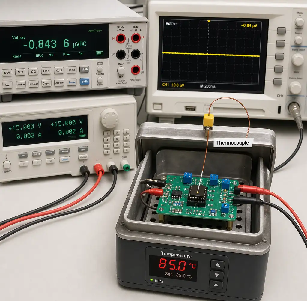 Op-amp offset voltage and temperature drift measurement setup with precision voltmeter
Modern zero-drift amplifiers use chopping or auto-zeroing to achieve offset below 10 µV with drift below 0.05 µV/°C—essentially eliminating DC errors. However, correction creates wideband noise and clock feedthrough spikes. Verify chopping frequency (typically 1-10 kHz) won't interfere with your signal spectrum.
Laser-trimmed bipolar devices like OPA187 achieve 25 µV maximum offset with 0.1 µV/°C drift—sufficient for many 16-bit systems—while delivering voltage noise below 5 nV/√Hz at lower cost.
Noise Analysis by Source Impedance
Op-amp noise appears as voltage noise (en) in series with input and current noise (in) flowing into terminals. Voltage noise adds directly; current noise through source impedance creates voltage: Vnoise = in × Rsource. The dominant source depends on source impedance.
Low source impedances (<1 kΩ) make voltage noise dominant. Choose bipolar stages achieving 1-3 nV/√Hz (LT1028, AD797). High impedances (>100 kΩ) flip the equation—1 pA/√Hz through 1 MΩ creates 1 µV/√Hz. Here, JFET or CMOS inputs with sub-femtoampere current noise dominate.
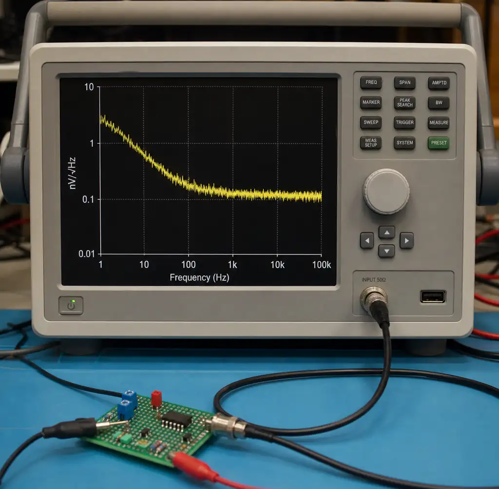 Voltage noise and current noise spectral density measurement on spectrum analyzer
Crossover impedance where both contribute equally: Rcrossover = en / in. For OPA1611 (3 nV/√Hz voltage, 5 fA/√Hz current), crossover occurs at 600 kΩ. Below this, voltage noise dominates; above it, current noise takes over.
Table 2: Noise-Optimized Selection by Source Impedance
| Source Impedance | Dominant Noise | Input Stage | Voltage Target | Current Target | Applications | Devices |
|---|---|---|---|---|---|---|
| <1 kΩ | Voltage (en) | Bipolar | <3 nV/√Hz | Not critical | Microphones, low-Z | LT1028, AD797 |
| 1-100 kΩ | Both | Bipolar/CMOS | <5 nV/√Hz | <10 fA/√Hz | RTD, load cells | OPA1612, AD8599 |
| 100 kΩ - 1 MΩ | Current (in) | JFET/CMOS | <20 nV/√Hz | <1 fA/√Hz | Photodiode, pH | OPA140, ADA4610 |
| >1 MΩ | Current (in) | CMOS | <50 nV/√Hz | <100 fA/√Hz | Piezo, ion | OPA128, ADA4528 |
Total integrated noise: Vnoise_total = en × √(BW × 1.57) for white noise. Don't forget 1/f noise below 10 Hz for DC applications.
Input Bias Current Considerations
Input bias current flows into terminals to bias internal transistors. This through source impedance creates DC error: Verror = Ibias × Rsource. For low impedances this remains negligible, but high-impedance sensors make bias current dominant.
Bipolar inputs exhibit 1-50 nA—acceptable below 10 kΩ but problematic beyond. Ten nA through 1 MΩ creates 10 mV error. JFET inputs reduce this to 1-100 pA, while CMOS achieves 1-10 pA. Zero-drift CMOS like OPA333 specify <50 pA maximum.
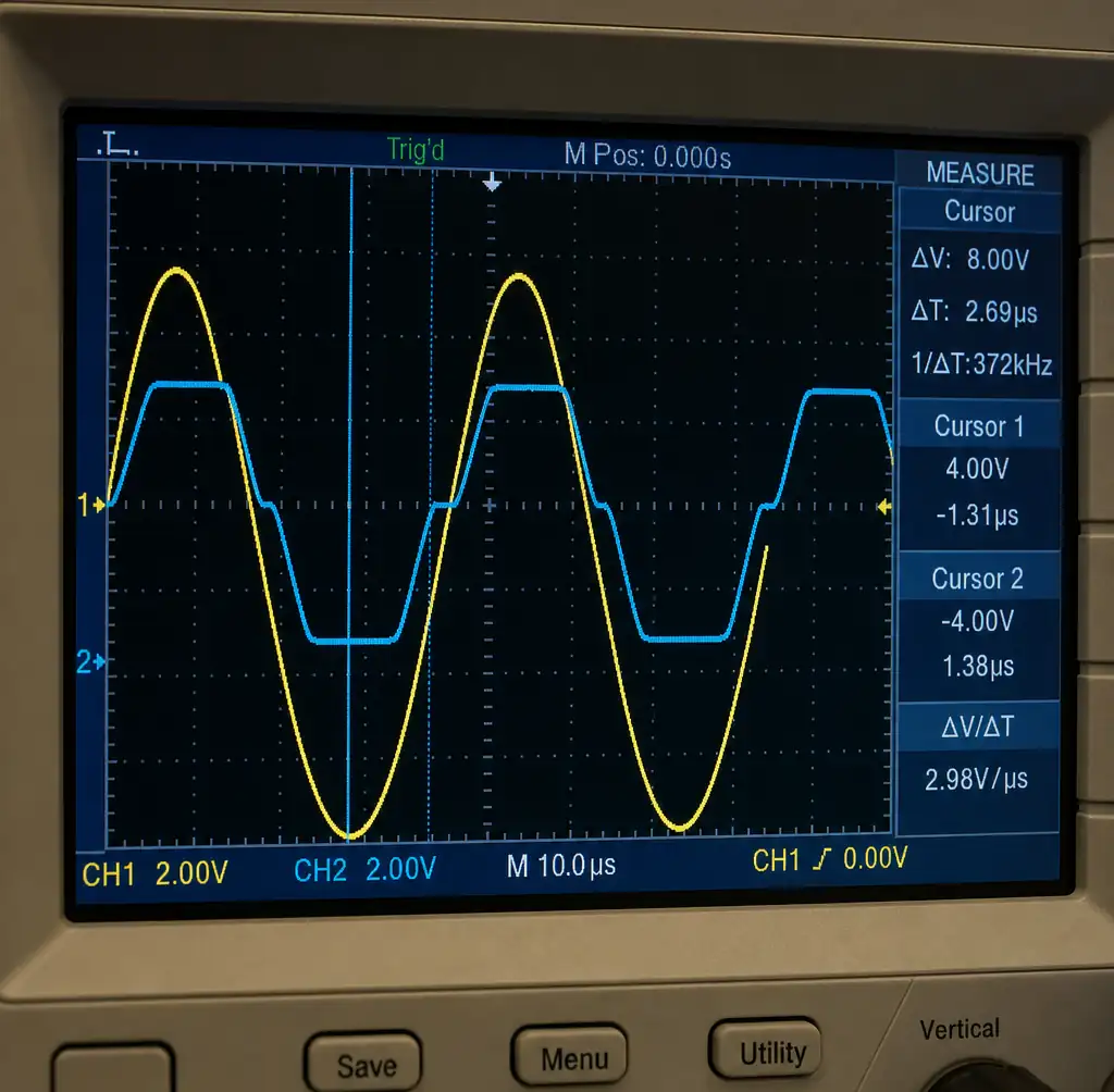 Oscilloscope capture showing op-amp slew rate limiting on sine wave output
When interfacing pH or ion-selective electrodes (>10 MΩ), even 1 pA creates error. These require electrometer-grade amplifiers like OPA128 (75 fA typical). Guard rings on PCB prevent board leakage from exceeding femtoampere-level bias current.
Zero-Drift vs Low-Noise Architectures
Choosing between zero-drift and traditional low-noise requires understanding the trade-off: zero-drift excels at DC accuracy but sacrifices wideband noise, while precision bipolar optimizes noise but accepts higher offset and drift.
Zero-drift achieves offset below 10 µV and drift below 0.05 µV/°C—an order of magnitude better than laser-trimmed bipolar. However, chopper op-amps exhibit broadband noise reaching 80-150 nV/√Hz—roughly 20-40x higher than best bipolar. For DC to 100 Hz, zero-drift delivers lower total noise due to eliminated 1/f noise. Above 1 kHz, bipolar wins.
Choose zero-drift for: DC-coupled applications across wide temperature ranges (thermocouples, precision references), high-gain DC amplification where offset × gain creates unacceptable error.
Choose low-noise bipolar for: Wideband applications with signal content above 1 kHz, ADC drivers requiring low integrated noise, transimpedance amplifiers, audio where 1/f noise is filtered.
Bandwidth and Stability
Gain-bandwidth product determines closed-loop bandwidth: BW ≈ GBW / Gain. An op-amp with 10 MHz GBW at gain 10 provides approximately 1 MHz -3dB bandwidth. Verify closed-loop bandwidth provides adequate phase margin (45-60°) to prevent peaking.
Slew rate limits output change speed. For sine waves: SR_required = 2π × f × Vpeak. A 100 kHz, 5Vpp sine requires SR = 1.57 V/µs minimum. Insufficient slew rate creates distortion.
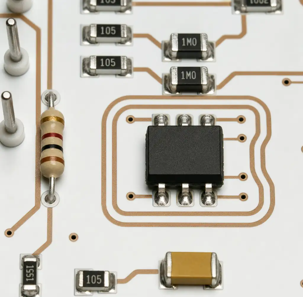 PCB layout showing guard ring implementation for high-impedance op-amp sensor interface
For precision DC applications, excess bandwidth hurts—amplifies more noise and increases RF susceptibility. Precision zero-drift op-amps limit bandwidth to 1-5 MHz to minimize noise while providing adequate settling.
Capacitive loads create additional poles, reducing phase margin. Three compensation strategies: (1) Isolation resistor (10-50Ω)—simple but creates DC error. (2) Feedback capacitor (1-10 pF)—preferred for precision. Place pole at fcomp = 1/(2π × Rf × Cf) approximately 5-10× below unity-gain bandwidth. (3) RC snubber for large loads (>1 nF).
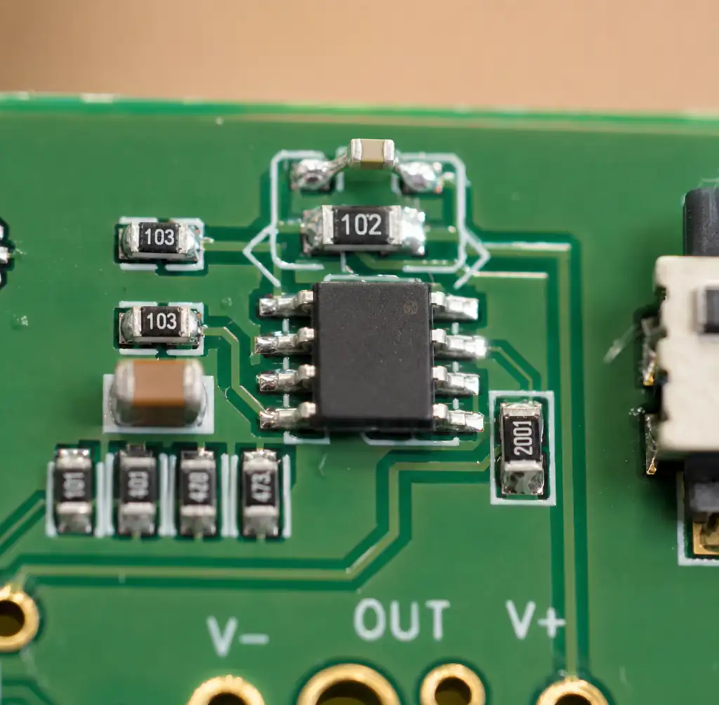 Feedback compensation capacitor placement on precision op-amp circuit board
When driving SAR ADCs, sampling capacitor presents dynamic load. TI's application note recommends characterizing worst-case load during acquisition.
FAQ
How do I calculate total output error from offset and bias current?
Total DC error: Verror_total = [Vos + (Ibias × Rsource)] × (1 + Rf/Ri) for non-inverting. For inverting: Verror = Vos × (1 + Rf/Ri) + Ibias × Rf. When source impedance exceeds 1 MΩ, bias current dominates; below 10 kΩ, offset dominates.
When should I choose zero-drift versus low-noise bipolar?
Choose zero-drift for DC-coupled applications across wide temperatures (thermocouples, references). Their <10 µV offset and <0.1 µV/°C drift eliminate calibration. Choose low-noise bipolar for wideband (>1 kHz) where 1-5 nV/√Hz outperforms zero-drift's 80-150 nV/√Hz.
How do I compensate capacitive loads without sacrificing accuracy?
Use feedback capacitor (1-10 pF) across Rf—preserves DC accuracy. Place pole at fcomp = 1/(2π × Rf × Cf) approximately 5-10× below unity-gain bandwidth. Verify with pulse response: <10% overshoot and clean settling within 2-3 time constants.
Can I use precision op-amps with single supplies?
Most support single-supply with rail-to-rail I/O. Verify input common-mode range—many require inputs 100-200 mV inside rails. Rail-to-rail inputs using CMOS exhibit crossover where offset degrades at mid-supply. Zero-crossover devices eliminate this.
What determines voltage versus current noise dominance?
Source impedance determines dominance. Below Rcross = en/in, voltage noise dominates; above it, current noise. For impedances below 10 kΩ, focus on voltage noise. For high-impedance sensors (>100 kΩ), current noise becomes critical.
How do I identify op-amp oscillation versus external noise?
True oscillation appears as clean, stable sine wave (1-100 MHz). It persists with grounded input. Use spectrum analyzer to identify frequency. Adding small feedback capacitor (1-2 pF) suppresses oscillation; external noise requires filtering.
What considerations apply to high-impedance sensor interfaces?
High impedance (>100 kΩ) makes bias current and current noise dominant. Select JFET/CMOS with <10 pA for impedances to 10 MΩ; use electrometer-grade (<100 fA) beyond. Guard rings prevent board leakage. Current noise creates voltage: Vn = in × Rsource.
Conclusion
Precision op-amp selection hinges on matching specifications to dominant error sources. For DC applications across wide temperatures, zero-drift eliminates offset and drift but accepts higher wideband noise. For wideband sensing above 1 kHz, low-noise bipolar delivers superior performance. Source impedance determines dominance—below 10 kΩ focus on voltage noise, above 100 kΩ prioritize low bias current.
Calculate total error including offset, drift at temperature extremes, noise integrated over bandwidth, and bias current through source impedance. Stability analysis prevents oscillation with capacitive loads—use feedback capacitors for precision.
Verify total DC error fits budget, integrated noise meets SNR, bandwidth provides phase margin (>45°), and settling meets timing. For sourcing, consult our product categories or request a quote. Hitop Tech Limited provides procurement services with technical support for precision analog requirements.