


Tunnel Diode Selection Guide 2026: High-Frequency & Low-Power Design
Key Takeaways (Quick Summary)
- Tunnel diodes provide negative differential resistance (NDR) enabling oscillation and amplification at frequencies >100 GHz from supply voltages <500 mV.
- Germanium (Ge) devices offer lower Vp (50–150 mV) and better noise performance for <20 GHz applications; GaAs devices provide lower capacitance (<0.5 pF) for millimeter-wave operation >40 GHz.
- Key selection parameters: Peak current (Ip), peak-to-valley ratio (Ip/Iv, ideally >10:1), negative resistance (Rn, typically -10Ω to -200Ω), and junction capacitance (Cj, determines fmax).
- Design challenges: Precise bias control (±20 mV), impedance matching in the negative resistance quadrant, thermal management, and preventing parasitic oscillations.
- Tunnel diodes remain relevant in 2026 for niche applications above 40 GHz or below 10 mW power consumption, but alternatives like RTDs, SiGe HBTs, and GaN HEMTs are replacing them in many traditional use cases.
Table of Contents
- What is a Tunnel Diode and Why It Matters in 2026
- Key Technical Parameters Explained
- Quantum Tunneling Operating Principle
- Performance Comparison: Tunnel Diode vs Conventional Diodes
- Application Scenarios and Design Examples
- Design Considerations and Common Pitfalls
- Tunnel Diode vs Modern Alternatives: 2026 Decision Framework
- FAQ
- Conclusion: Is a Tunnel Diode Right for Your 2026 Design?
1. What is a Tunnel Diode and Why It Matters in 2026
A tunnel diode is a heavily doped P-N junction that exhibits negative differential resistance (NDR) in its forward-biased region. First demonstrated by Leo Esaki in 1957 (Nobel Prize, 1973), it leverages quantum mechanical tunneling to achieve switching speeds in the picosecond range—making it invaluable for high-frequency oscillators, mixers, and low-power detectors.
Why it still matters in 2026:
- Frequency: Operates at >100 GHz—beyond the practical limit of most conventional transistors.
- Power: Consumes <10 mW at 100 GHz—unmatched by active transistor designs.
- Simplicity: A single two-terminal device oscillates without complex transistor biasing.
- Reliability: No inherent wear-out mechanism (no minority carrier injection degradation).
The 2026 reality: Tunnel diodes are no longer a mainstream component, but remain irreplaceable in defense radar, millimeter-wave instrumentation, aerospace downlinks, and cryogenic applications where low noise and ultra-low power are non-negotiable.
2. Key Technical Parameters Explained
| Parameter | Symbol | Typical Range (Ge) | Typical Range (GaAs) | Design Impact |
|---|---|---|---|---|
| Peak current | Ip | 0.1–50 mA | 1–20 mA | Sets operating bias point |
| Peak voltage | Vp | 50–150 mV | 150–300 mV | Defines minimum supply voltage |
| Valley current | Iv | 0.02–10 mA | 0.2–4 mA | Ip/Iv ratio (3:1 to 15:1) determines NDR width |
| Negative resistance | Rn | -10Ω to -100Ω | -20Ω to -200Ω | Determines Q-factor and gain potential |
| Junction capacitance | Cj | 1–20 pF | 0.1–0.5 pF | fmax ≈ 1/(2π·Rn·Cj) |
| Series resistance | Rs | 0.5–5Ω | 1–3Ω | Degrades Rn at high frequencies |
| Temp coefficient (Ip) | — | +0.5%/°C | +0.3%/°C | Requires compensation in precision designs |
Critical design rules:
- Ip/Iv ratio > 10:1 provides robust oscillator start-up margin.
- Cj < 1 pF required for operation above 20 GHz (GaAs recommended).
- Vp + Iv·Rs determines actual circuit operating voltage—verify with the manufacturer's I-V curve.
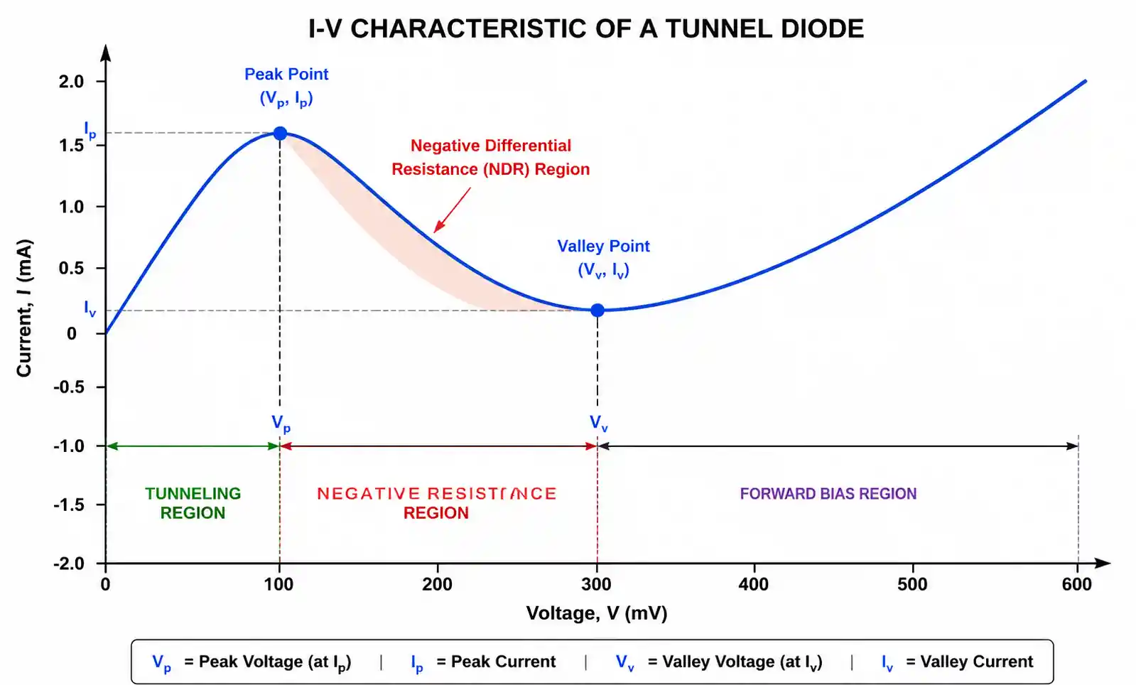
3. Quantum Tunneling Operating Principle
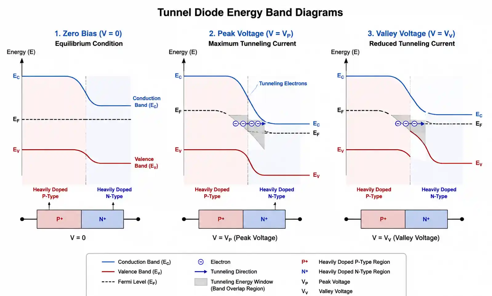
The tunnel diode's unique I-V characteristic stems from quantum mechanical tunneling—not classical carrier injection.
Why tunneling occurs: Doping concentrations >10¹⁹ cm⁻³ reduce the depletion width to approximately 10 nm—thin enough for electrons to tunnel through the potential barrier.
I-V Curve Four Regions:
| Region | Bias Range | Physical Mechanism | Circuit Utility |
|---|---|---|---|
| 0 → Vp | 0 to 50–300 mV | Increasing tunneling states available | Rising current, positive resistance |
| Vp → Vv | Vp to 200–500 mV | Band misalignment reduces tunneling probability | Negative resistance—oscillation/amplification |
| Vv → forward | >Vv | Conventional injection current dominates | Standard diode behavior (rarely used) |
| Reverse bias | Negative | Zener-like breakdown | Minimal use |
Key insight: The NDR region is purely quantum mechanical with femtosecond response time—no charge storage, no reverse recovery, no carrier transit delay.
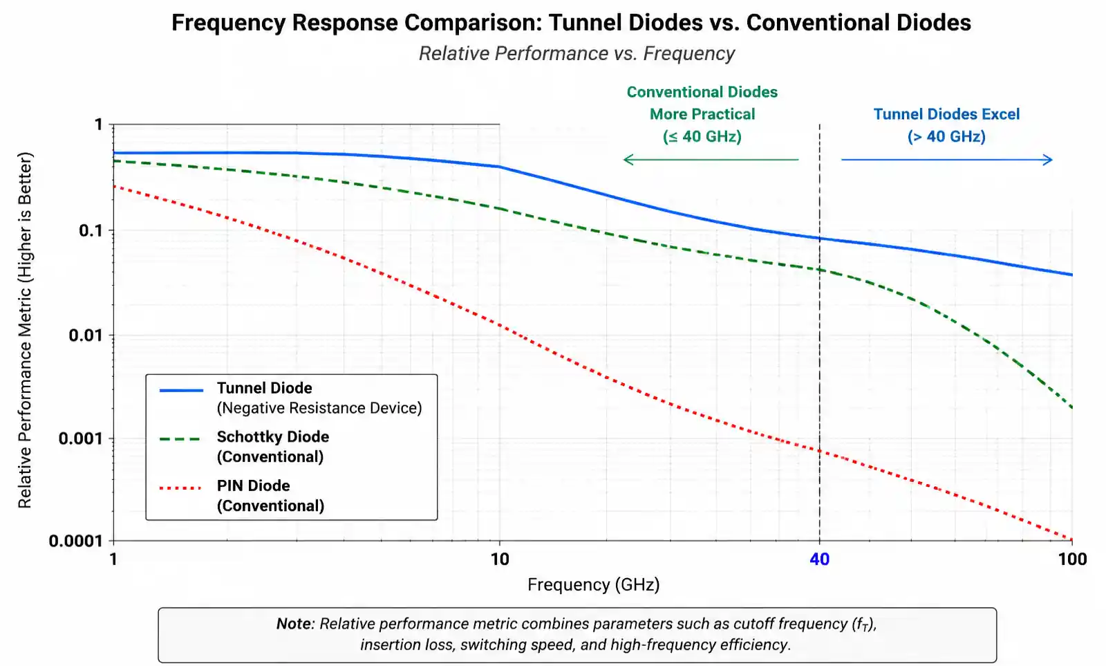
4. Performance Comparison: Tunnel Diode vs Conventional Diodes
| Parameter | Tunnel Diode | Schottky | PIN | Varactor |
|---|---|---|---|---|
| Forward voltage | 50–300 mV | 200–500 mV | 600–1000 mV | N/A |
| Switching speed | <1 ps | 10–100 ps | 1–10 ns | 10–100 ps |
| Max frequency | >100 GHz | 20–50 GHz | 1–10 GHz | 50–100 GHz |
| Negative resistance | Yes | No | No | No |
| Noise figure (dB) | 2–4 | 3–6 | 6–10 | N/A |
| Power handling | <100 mW | 1–10 W | 10–100 W | <1 W |
| Temp stability | Moderate (±0.5%/°C) | Good (±0.1%/°C) | Good | Fair |
When to choose tunnel diode:
- Operating frequency >40 GHz
- Power consumption must be <10 mW with reasonable NF
- Simplest possible oscillator topology required
- Cryogenic or space operation (no carrier freeze-out issues)
When NOT to choose tunnel diode:
- Frequency <20 GHz (Schottky or transistor designs are simpler)
- Power handling >100 mW required
- Wide temperature range without compensation (−40°C to +125°C)
- Cost-sensitive or high-volume production
5. Application Scenarios and Design Examples
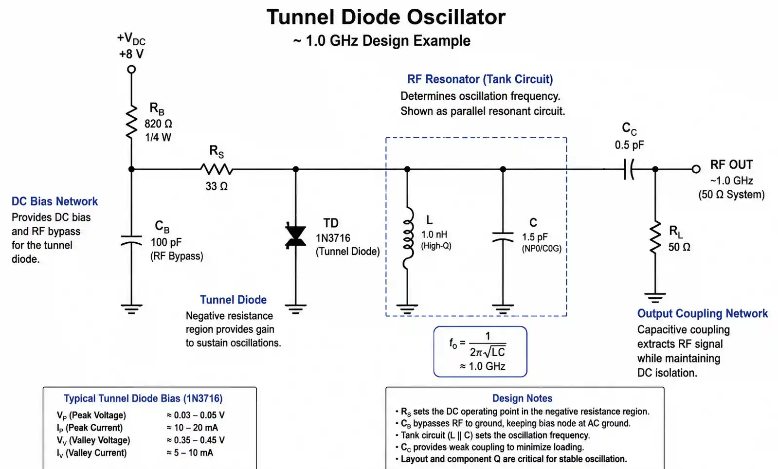
5.1 High-Frequency Oscillators (10–100 GHz)
Circuit: Tunnel diode + DC bias + RF resonator (cavity, microstrip, or dielectric resonator) + output coupling.
Design equation: Oscillation condition = |Rn| > Rload + Rresonator (at operating frequency).
Typical specs: GaAs tunnel diode, Ip = 5–10 mA, Rn = -50Ω, Cj = 0.2 pF → fmax ≈ 1/(2π × 50 × 0.2×10⁻¹²) ≈ 16 GHz. With careful layout, practical oscillators reach 40–60 GHz.
5.2 Low-Noise Amplifiers (5–40 GHz)
Tunnel diode amplifiers can achieve NF < 3 dB at frequencies where conventional transistors struggle. The key challenge is stability—the negative resistance must be carefully controlled.
Design approach: Use a circulator or directional coupler to separate input and output (reflection amplifier topology). Bias slightly below Vp for lowest noise.
5.3 Ultra-Fast Detectors and Mixers
Zero charge storage makes tunnel diodes ideal for detecting pulses <10 ps and mixing signals to millimeter-wave frequencies. Operate near the valley point (Iv) for square-law detection with minimal bias current—critical for energy-harvesting and remote sensor applications.
5.4 Application Parameter Table
| Application | Frequency | Device Type | Bias Point | Key Challenge |
|---|---|---|---|---|
| Local oscillator | 20–100 GHz | GaAs, Ip=1–10 mA | Near Vp | Phase noise, temperature stability |
| LNA | 5–40 GHz | Ge, Ip=5–20 mA | Below Vp | Stability, gain-BW trade-off |
| Detector | DC–60 GHz | Ge/GaAs, Ip=0.5–5 mA | Near Iv | Sensitivity, dynamic range |
| Pulse generator | DC–10 GHz | Ge, Ip=10–50 mA | NDR region | Rise time, pulse fidelity |
6. Design Considerations and Common Pitfalls
6.1 Bias Network Design
- Bias must be stable to ±20 mV—use low-impedance source (<5Ω).
- Series resistance in bias path adds to Rs and degrades Rn.
- For temperature-sensitive applications, use compensating diode or active bias control.
6.2 Impedance Matching
- Tunnel diode impedance is low (10–50Ω) and negative—Smith chart in the negative resistance quadrant is essential.
- Load must present positive resistance less than |Rn| at oscillation frequency.
6.3 Stability and Parasitic Oscillations
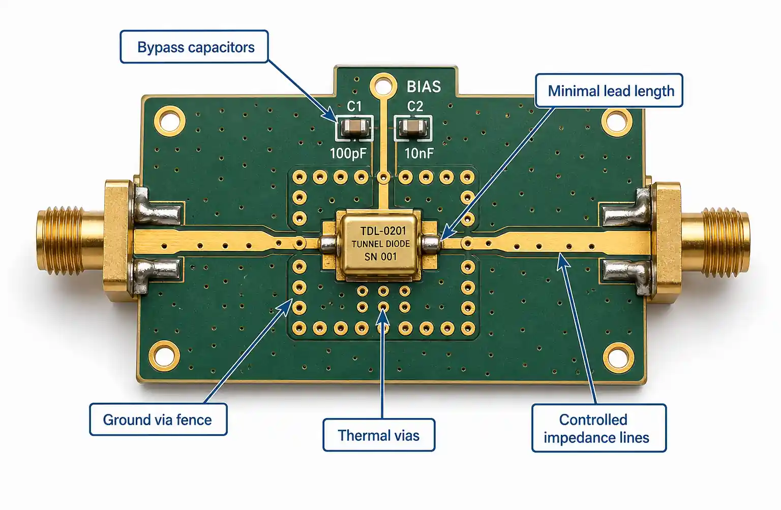
- Any circuit with net negative resistance at any frequency will oscillate.
- Best practices: Minimize lead inductance (flip-chip or direct die attach), use multiple ground vias, simulate with parasitic extraction.
6.4 Thermal Management
- Junction temperature can exceed 100°C at 50 mW dissipation.
- Use thermal vias under device; consider copper coin mounting >30 mW.
- Thermal runaway risk: If temperature raises bias current into positive resistance region, power dissipation increases further.
6.5 Common Mistakes to Avoid
- Operating too close to Vp (maximum sensitivity to bias drift)
- Neglecting package inductance in high-frequency designs
- Using high-impedance bias supplies (allow operating point shift)
- Insufficient bypassing (creates low-frequency instability loops)
- Attempting to parallel tunnel diodes (negative resistance makes this unstable)
7. Tunnel Diode vs Modern Alternatives: 2026 Decision Framework
The tunnel diode faces increasing competition from modern semiconductor technologies. Here's how they compare in 2026:
| Technology | Frequency | Power | Maturity | Cost | Best Application |
|---|---|---|---|---|---|
| Tunnel Diode | >100 GHz | <10 mW | Mature | $$$ | Ultra-low-power mm-wave oscillators |
| RTD (Resonant Tunneling Diode) | >1 THz | <5 mW | Emerging | $$$$ | THz imaging, ultra-high-speed logic |
| SiGe HBT | 50–100 GHz | 50–200 mW | Mature | $$ | Microwave amplifiers, VCOs |
| GaN HEMT | 10–40 GHz | 1–10 W | Mature | $$$ | Power amplifiers, radar transmitters |
| InP HEMT | 100–300 GHz | 10–100 mW | Maturing | $$$$ | Millimeter-wave receivers |
| CMOS (advanced nodes) | 30–60 GHz | 10–50 mW | Mature | $ | Consumer mm-wave, 5G/6G |
Decision flow for 2026:
- Frequency > 100 GHz? → Consider tunnel diode or RTD.
- Frequency 40–100 GHz + Power <10 mW? → Tunnel diode is still competitive.
- Frequency 40–100 GHz + Power >50 mW? → SiGe HBT or InP HEMT.
- Frequency <40 GHz → Use SiGe HBT, GaN HEMT, or CMOS—simpler, cheaper, better integration.
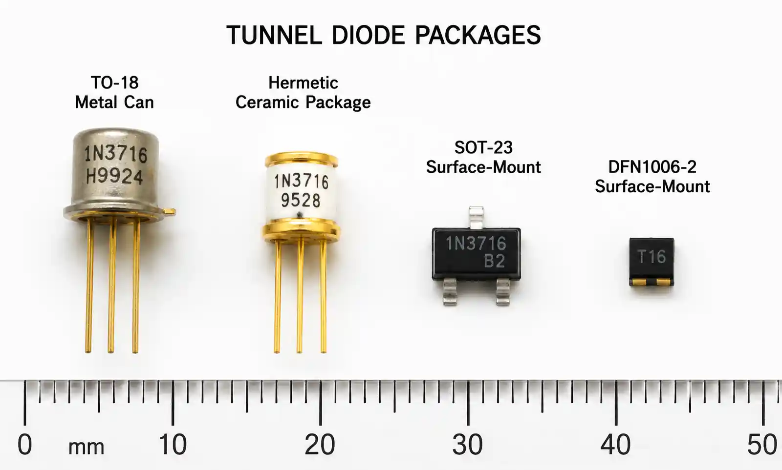
Sourcing note: Tunnel diodes are available from specialized suppliers including MACOM, Microsemi (now Microchip) , and select defense-oriented semiconductor houses. Lead times: 12–26 weeks for custom specifications. Standard germanium devices (1N3712 series) may be available from distributors like Digi-Key or Mouser from legacy inventory.
8. FAQ
What is the main advantage of a tunnel diode over a regular diode?
Negative differential resistance enables oscillation/amplification without active devices, plus sub-picosecond switching due to quantum tunneling. No other two-terminal device provides gain at >100 GHz from <500 mV.
Why aren't tunnel diodes more common?
Narrow operating range (requires precise bias), low power handling (<100 mW), temperature sensitivity (±0.5%/°C), and higher cost than alternatives. Below 20 GHz, modern transistors and Schottky diodes offer better overall value.
What materials are used?
- Germanium (Ge): Lower Vp (50–150 mV), higher Ip/Iv ratio, better NF—preferred for <20 GHz.
- Gallium arsenide (GaAs): Lower Cj (<0.5 pF), higher frequency (to 200 GHz)—preferred for >40 GHz.
How do I prevent unwanted oscillations?
Minimize parasitic inductance with short leads and proper PCB layout. Use low-inductance SMT bypass caps adjacent to the device. Simulate with accurate parasitics. In amplifier designs, use isolators or circulators for stability.
Can tunnel diodes be used in automotive/industrial applications?
Yes, with temperature compensation. The ±0.5%/°C coefficient means a 100°C swing shifts operating point significantly—use active bias compensation or oven-controlled environments for precision applications.
What is the typical lifespan?
100,000 hours when operated within limits. No inherent wear-out mechanism—failure modes are mechanical (bond wire fatigue, package seal) or electromigration from over-current.
Are there modern alternatives?
RTDs offer THz capability with improved peak-to-valley ratios. SiGe HBT and GaN HEMT now reach many frequencies where tunnel diodes were previously required, with better power handling and integration. Tunnel diodes remain competitive only for ultra-low-power (<10 mW) applications above 40 GHz.
How do I source tunnel diodes?
Contact specialized semiconductor houses serving defense/aerospace markets. Distributors occasionally stock legacy germanium devices (1N3712 series). Lead times: 12–26 weeks.
9. Conclusion: Is a Tunnel Diode Right for Your 2026 Design?
Choose a tunnel diode when:
- Operating frequency >40 GHz and power consumption must be <10 mW
- You need the simplest possible oscillator topology
- Application is in defense, aerospace, instrumentation, or cryogenics where cost is secondary to performance
- You can tolerate 12–26 week lead times and specialized sourcing
Choose alternatives when:
- Frequency <40 GHz (use SiGe HBT, GaN HEMT, or CMOS)
- Power handling >100 mW required
- Wide temperature range without compensation (−40°C to +125°C)
- Cost-sensitive or high-volume production
Key design priorities for tunnel diode success:
- Characterize actual devices—manufacturing variations shift Vp by ±30 mV and Ip by ±20%
- Simulate with parasitic extraction—bond wire inductance is critical above 10 GHz
- Design bias for stability—use low-impedance sources and temperature compensation
- Validate across temperature extremes—tunnel diodes are temperature-sensitive
- Plan for procurement—lead times are longer than standard components
For further technical support, consult manufacturer application notes and datasheets with complete I-V characterization data. In critical applications, prototype testing across temperature and supply voltage extremes is essential before production commitment.