



TVS Diode Selection for ESD and Surge Protection
Modern electronic systems face constant threats from electrostatic discharge (ESD) events and voltage transients. A single 15kV ESD strike can destroy unprotected semiconductor junctions in microseconds, while lightning-induced surges on power or communication lines can cascade through entire systems. After qualifying protection circuits for automotive and industrial applications over the past decade, I've seen how proper TVS diode selection prevents field failures that cost 10-100× more than the component itself.
This guide provides a structured approach to selecting TVS diodes based on circuit voltage, transient characteristics, and application standards. You'll learn how to calculate clamping voltage margins, avoid common specification traps, and apply automotive-grade versus industrial-grade protection appropriately.
Table of Contents
- How TVS Diodes Protect Circuits
- Critical TVS Diode Parameters
- TVS Diode Selection Process
- Automotive vs Industrial TVS Requirements
- Common TVS Selection Mistakes
- PCB Layout Considerations
- FAQ
- Conclusion
How TVS Diodes Protect Circuits
TVS (Transient Voltage Suppressor) diodes operate as voltage clamps. During normal operation, they remain non-conductive with only picoampere-level leakage. When a transient exceeds the breakdown voltage, the TVS enters avalanche mode within nanoseconds, shunting surge current to ground while limiting voltage to a safe clamping level.
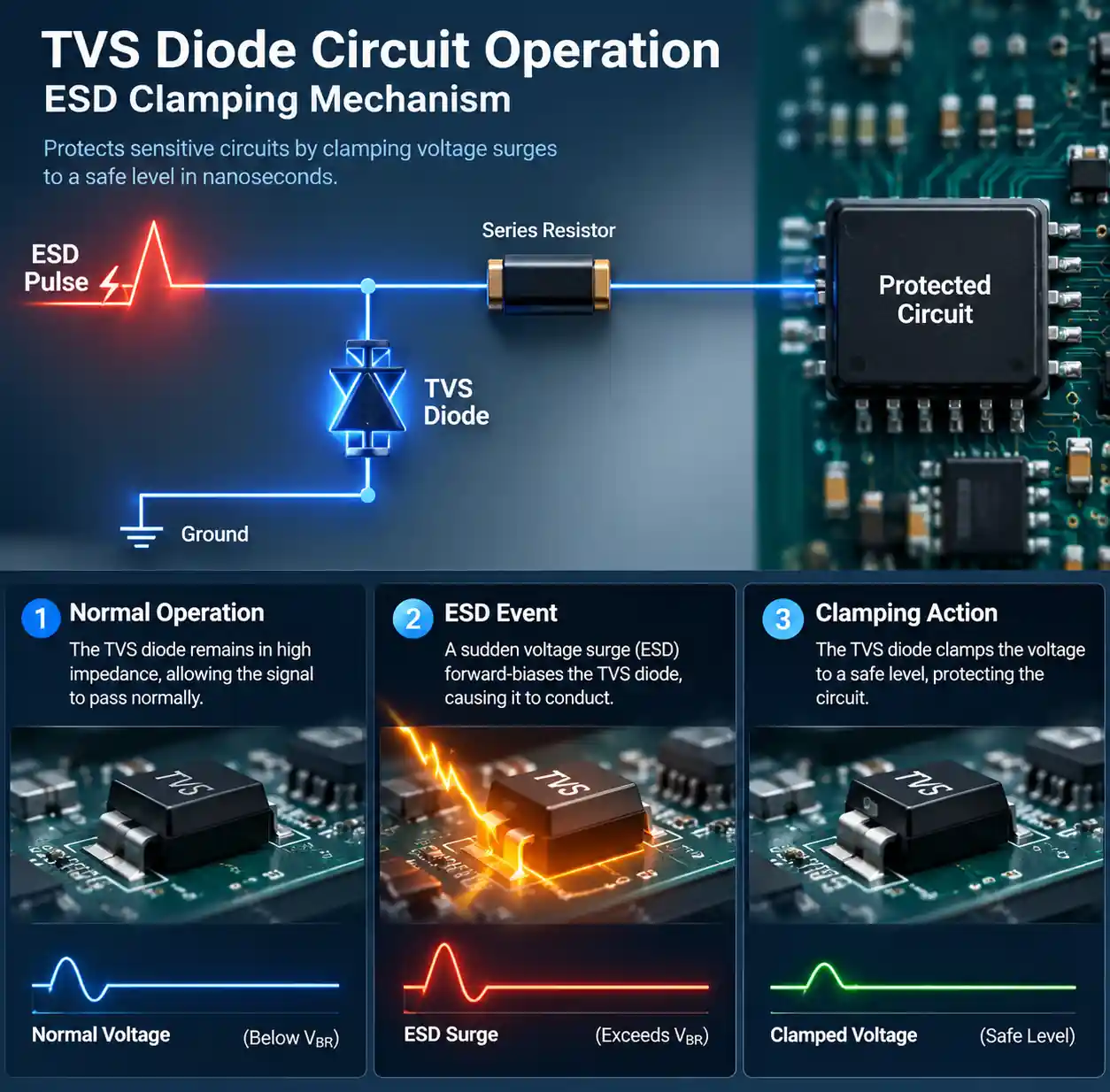 TVS diode circuit operation showing ESD clamping mechanism
Unlike MOVs (metal oxide varistors) that degrade with repeated surges, silicon TVS diodes maintain consistent clamping performance over thousands of ESD events. Their sharp breakdown characteristic and sub-nanosecond response time make them ideal for protecting fast digital interfaces where signal integrity matters.
The protection mechanism works through three distinct voltage regions. Below the standoff voltage (VRWM), the TVS behaves as a high-impedance element with minimal circuit loading. Between VRWM and breakdown voltage (VBR), leakage current rises but remains in the microampere range. Above VBR, the TVS conducts heavily, with clamping voltage (VC) determined by peak pulse current (IPP).
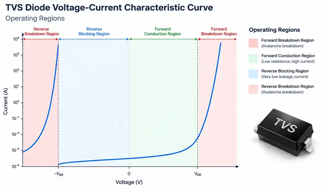 TVS diode voltage-current characteristic curve showing operating regions
When a transient voltage appears on a protected line, the TVS responds in picoseconds to low nanoseconds depending on junction capacitance and package parasitics. This speed far exceeds semiconductor damage thresholds—gate oxides fail in 10-50 nanoseconds under overvoltage stress, so sub-nanosecond TVS response provides adequate protection margin.
The energy absorption capacity of a TVS depends on its silicon junction area and thermal design. During an ESD event lasting 1-100 microseconds, the TVS must absorb the pulse energy without exceeding its maximum junction temperature (typically 175°C). Properly sized TVS diodes handle this thermal pulse, cool down between events, and protect through thousands of ESD strikes without degradation.
Bidirectional versus unidirectional TVS diodes serve different applications. Unidirectional types protect DC power rails and circuits where voltage polarity remains constant—they clamp overvoltage in one direction while acting as a forward-biased diode (low impedance) in the reverse direction. Bidirectional TVS diodes contain two junctions in series opposition, clamping voltage swings in both positive and negative directions. Use bidirectional TVS for AC signals, differential data pairs (USB, CAN, Ethernet), and any interface where signal ground reference might shift or reverse polarity transients occur.
Critical TVS Diode Parameters
Understanding TVS specifications enables proper device selection and avoids the common trap of specifying based solely on breakdown voltage.
Standoff voltage (VRWM or VWM) represents the maximum continuous voltage the TVS can withstand while remaining non-conductive. Leakage current stays below specified limits (typically 1-10 μA) at and below VRWM. Select VRWM at least 10-30% above your maximum normal operating voltage to account for supply tolerance, ripple, and transient variations. For a 5V rail with ±5% tolerance (4.75-5.25V), specify VRWM ≥ 5.8V to ensure the TVS remains off during normal operation.
Breakdown voltage (VBR) specifies the voltage at which the TVS begins conducting substantial current, typically defined at 1 mA test current. Datasheets list VBR with tolerance—for example, "6.4V ±5%"—meaning actual breakdown spans 6.08V to 6.72V. This tolerance matters for worst-case analysis: the highest VBR unit determines your maximum clamping voltage.
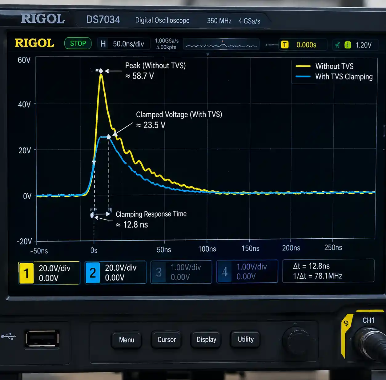 ESD waveform capture showing TVS diode clamping response time
Clamping voltage (VC) represents the voltage across the TVS when conducting peak surge current. This parameter determines whether your protected IC survives. VC must remain below the IC's absolute maximum rating with adequate margin—typically 20-30% to account for ground bounce, ringing, and measurement uncertainty. For a 3.3V I/O buffer with 5V absolute maximum rating, specify a TVS with VC ≤ 4.0V at the expected surge current.
Clamping voltage increases with surge current magnitude. A TVS rated at VC = 9.2V at IPP = 1A might clamp at 11V when conducting 5A. Check the datasheet's clamping voltage versus current curve and use the current level matching your transient specification (often derived from IEC 61000-4-2 or IEC 61000-4-5 standards).
Peak pulse current (IPP) specifies the maximum surge current the TVS can safely conduct without damage, typically tested with an 8/20 μs waveform (8 μs rise time, 20 μs decay to 50% peak). Common ratings range from 1A to over 100A for small signal devices, with power TVS diodes reaching thousands of amperes. Calculate the expected surge current based on your application's transient source impedance and energy level, then select a TVS with IPP rating providing at least 20-30% margin.
Junction capacitance (CJ) becomes critical for high-speed data interfaces. TVS capacitance appears in parallel with the protected signal line, creating a low-pass filter that attenuates high-frequency signal components. For USB 2.0 (480 Mbps), specify CJ < 5 pF per line. Gigabit Ethernet and USB 3.0 (5 Gbps) require ultra-low capacitance TVS arrays with CJ < 0.5 pF to avoid eye diagram closure. Low-speed interfaces (RS-232, I²C, 10 Mbps Ethernet) tolerate 50-200 pF without signal degradation.
Leakage current (IR) at VRWM should remain low enough not to affect circuit operation. Most TVS diodes specify IR < 1 μA at room temperature, rising to 10-50 μA at 125°C due to semiconductor thermal generation. For high-impedance nodes or battery-powered systems where every microampere matters, verify leakage at maximum operating temperature before finalizing selection.
TVS Diode Selection Process
A systematic approach prevents under-protection (IC damage) and over-protection (unnecessary cost, signal degradation) while ensuring compliance with applicable standards.
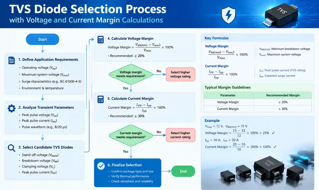 TVS diode selection process flowchart with voltage and current margin calculations
Step 1: Identify circuit operating voltage and tolerance. Determine maximum normal voltage including supply tolerance, ripple, and transient overshoot. For a 12V automotive rail with -40% / +40% transients per ISO 7637-2 (7.2V to 16.8V), use Vmax = 16.8V as the baseline.
Step 2: Select standoff voltage. Choose VRWM ≥ Vmax × 1.1 to maintain margin. For the 16.8V example, specify VRWM ≥ 18.5V. Standard TVS diodes come in discrete VRWM values (often following 10% increments), so you'd select the next available rating—typically 20V or 22V.
Step 3: Verify IC absolute maximum rating. Consult the protected IC's datasheet for absolute maximum voltage on the protected pin. Most 3.3V I/O tolerates 5-5.5V absolute maximum; 5V logic typically handles 7-8V. Build in 20-30% margin between TVS clamping voltage and IC rating to account for inductance-induced voltage spikes in the protection path.
Step 4: Calculate expected surge current. For ESD protection per IEC 61000-4-2, estimate Isurge using the standard's current waveform and any series resistance in your circuit. Contact discharge at 8 kV produces roughly 30A peak current with fast rise time. For surge immunity per IEC 61000-4-5, 1 kV coupled through the specified network produces current determined by the network impedance—typically 10-30A for industrial equipment.
If series resistance exists (connector contact resistance, trace impedance, current-limiting resistors), it reduces the current through the TVS: ITVS = (Vtransient - VC) / Rseries. A 10Ω series resistor drops substantial voltage during an ESD event, significantly reducing the TVS current requirement.
Step 5: Select TVS with adequate IPP rating. Choose a TVS rated for IPP ≥ Isurge × 1.3 margin factor. For the 30A ESD case, specify IPP ≥ 40A.
Step 6: Verify clamping voltage at calculated surge current. Using the selected TVS's datasheet curves, find VC at your Isurge level. Confirm VC + (Isurge × Lparasitic × di/dt) < IC absolute maximum rating × 0.75. The inductance term accounts for voltage spikes caused by parasitic inductance in PCB traces and TVS leads—typically 5-20 nH total, producing 5-20V additional spike for fast ESD edges.
Step 7: Check capacitance for signal integrity. For data interfaces, verify CJ < maximum allowable capacitance derived from rise time or frequency requirements. Use the rule: Cmax ≈ trise / (10 × Z0), where Z0 is characteristic impedance. For a 2 ns rise time on 50Ω transmission line, Cmax ≈ 4 pF. Lower capacitance TVS diodes cost more and have lower IPP ratings, so balance signal integrity needs against protection capability.
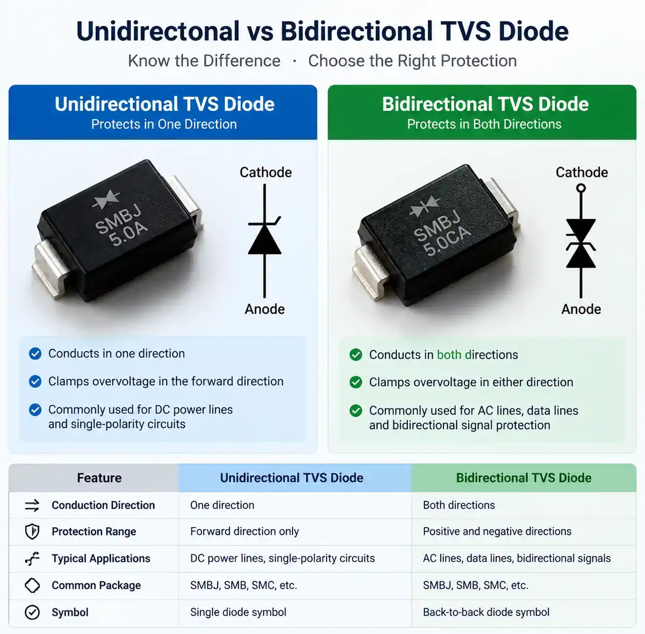 Unidirectional vs bidirectional TVS diode comparison chart
Step 8: Consider bidirectional versus unidirectional configuration. Use bidirectional TVS for AC-coupled signals, differential pairs without defined ground reference, or any interface where negative transients can occur. Power rails protecting against positive-only transients can use unidirectional types for lower capacitance and potentially lower cost.
Automotive vs Industrial TVS Requirements
Different application domains specify distinct transient immunity standards that directly influence TVS selection.
Automotive applications must survive the transients defined in ISO 7637-2 (conducted transients on 12V power lines) and ISO 7637-3 (coupled transients on signal lines). Test pulses include load dump (up to +100V for 400 ms when alternator disconnects under load), jump start (+24V sustained), reverse battery (-14V), and various inductive switching transients.
For 12V automotive circuits, typical TVS specifications include:
- VRWM = 20-24V (handles 16.8V load dump with margin)
- IPP = 50-100A minimum (load dump energy varies with alternator size)
- VC < 35-40V (protects integrated circuits rated for 40-45V absolute maximum)
- AEC-Q101 qualified for temperature cycling (-40°C to +150°C) and moisture sensitivity
The long-duration load dump (100V for 400 ms) requires attention to average power dissipation, not just peak current. A series resistor or inductor often precedes the TVS to limit continuous current during extended transients, preventing thermal runaway. Calculate average power: Pavg = (Vload_dump - VC) × Iclamp × duty_cycle, and verify the TVS's thermal impedance keeps junction temperature below rating.
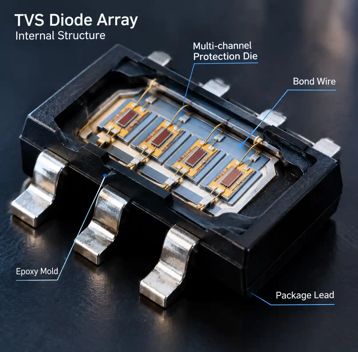 TVS diode array internal structure showing multi-channel protection die
Industrial equipment typically follows IEC 61000-4-5 (surge immunity) and IEC 61000-4-4 (electrical fast transient) standards. Surge testing injects 0.5 kV to 4 kV pulses through defined coupling networks simulating lightning-induced transients on power and communication lines. EFT testing applies bursts of 0.5-4 kV fast pulses (5 ns rise time, 50 ns width) at 5-100 kHz repetition rate.
Industrial TVS selection prioritizes:
- VRWM matched to the input voltage range (24V industrial bus → 30V VRWM; 48V → 60V VRWM)
- IPP ratings for 1-4 kV surges after accounting for series impedance (2Ω coupling resistance per IEC standard reduces current versus direct coupling)
- Multi-strike capability since industrial equipment must survive repeated surge events over 20+ year service life
- Often integrated into TVS arrays protecting multiple lines (8-channel, 16-channel arrays for industrial I/O cards)
Consumer electronics ESD protection emphasizes IEC 61000-4-2 compliance at 4-8 kV contact discharge levels. USB ports, HDMI connectors, and external interfaces require TVS arrays with low capacitance (<2 pF per line for high-speed data) yet adequate IPP (30-50A peak) to handle 8 kV contact discharge through minimal series impedance. Space constraints favor multi-channel TVS arrays in compact packages—single SOT23-6 or DFN packages protecting four differential pairs.
Common TVS Selection Mistakes
Field experience reveals recurring errors that compromise protection or unnecessarily increase cost and complexity.
Mistake 1: Selecting TVS by breakdown voltage alone. Engineers often match VBR to supply voltage without considering that VRWM must exceed operating voltage. A 5V rail requires VRWM > 5.5V, which corresponds to VBR ≈ 6.0-6.5V and VC ≈ 9-10V—significantly higher than the protected voltage. Selecting a 5V breakdown TVS results in continuous leakage or premature conduction during normal operation.
Mistake 2: Ignoring clamping voltage versus current relationship. Specifying IPP = 30A but only checking VC at the datasheet test condition (often 1A) leads to under-protection. VC increases 30-50% between 1A and 30A for typical TVS diodes. Always verify VC at your actual expected surge current, not the datasheet headline rating.
Mistake 3: Overlooking parasitic inductance effects. The voltage across an inductance equals L × di/dt. During ESD events with di/dt = 10A/ns, even 10 nH trace inductance generates 100V spike. This spike adds to the TVS clamping voltage: Vtotal = VC + Ltrace × di/dt. Place TVS as close as physically possible to the protected pin and use wide, short traces to minimize inductance. Calculate worst-case total voltage including inductive spike to ensure IC survival.
Mistake 4: Using high-capacitance TVS on sensitive interfaces. Protecting a USB 3.0 SuperSpeed lane (5 Gbps) with a 50 pF TVS virtually guarantees signal integrity failure. The capacitance creates a low-pass filter with -3 dB point well below the signal bandwidth, causing eye closure and bit errors. Pay the premium for low-capacitance TVS arrays (<0.5 pF) or accept that the interface won't meet electrical specifications.
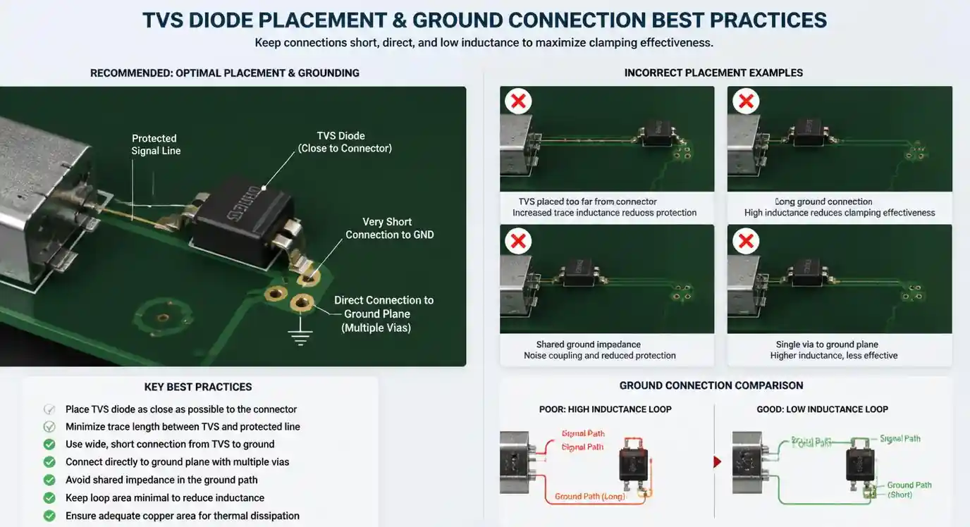 PCB layout best practices for TVS diode ground connection and placement
Mistake 5: Forgetting temperature effects. VBR and VRWM drift with temperature, typically -2 to -3 mV/°C for silicon TVS diodes. A TVS with VRWM = 5.5V at 25°C drops to approximately 5.2V at 125°C. If your circuit operates at 5.3V maximum at high temperature, you've lost your margin and the TVS begins conducting continuously. Account for temperature coefficient when calculating VRWM margin requirements.
Mistake 6: Series resistor creates secondary problem. Adding a series resistor to limit TVS current during surges seems logical but creates voltage drop during normal operation. For power lines carrying continuous current, Vdrop = Iload × Rseries wastes power and reduces available voltage. Series resistors work well for signal lines with minimal DC current but complicate power rail protection. Consider active clamping or crow-bar circuits for power lines requiring both high current delivery and transient protection.
PCB Layout Considerations
Even a perfectly specified TVS fails to protect if PCB layout introduces excessive parasitic inductance or ground impedance.
Placement rules: Mount the TVS directly at the connector or entry point where the transient enters. Every millimeter of trace between the connector pin and TVS anode adds inductance that increases total clamping voltage. For USB connectors, place the TVS array within 5mm of the connector pins. For board-to-board connectors in industrial equipment, place TVS immediately adjacent to the connector.
Ground connection architecture: The TVS's ground connection must provide a low-impedance path back to the transient source or chassis ground. Use short, wide ground traces or, ideally, direct via-in-pad connections to a ground plane. Multiple vias in parallel (2-4 vias for high-current TVS) reduce ground inductance below 1 nH, minimizing ground bounce during surge events.
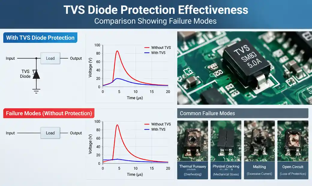 TVS diode protection effectiveness comparison showing failure modes
Trace width and routing: Run wide traces (≥20 mil for signal-level protection, ≥50 mil for power line protection) to reduce series resistance and inductance. Avoid long parallel runs near sensitive analog circuits—the transient current pulse couples magnetically into nearby traces. Route protected and unprotected signals on separate PCB layers or with ground plane separation when possible.
Kelvin connection for shared ground: When multiple TVS devices share a ground point, use Kelvin connections to prevent one TVS's surge current from creating voltage drop in another TVS's ground path. Each TVS should have dedicated ground connections joining at a single, low-impedance star point—typically a via cluster to a ground plane directly beneath the protection array.
Test points and inspection: Include test points on both sides of TVS diodes to enable in-circuit verification of TVS function. After ESD or surge testing, measure forward voltage drop to confirm the TVS hasn't failed short, and measure leakage at VRWM to verify it hasn't degraded. Failed TVS diodes usually fail short circuit (protective failure mode) rather than open, so the protected IC survives but the TVS requires replacement.
FAQ
Can I parallel multiple TVS diodes to increase current handling?
Yes, but unequal breakdown voltages cause current imbalance. Due to VBR tolerance (typically ±5%), the lowest-VBR unit conducts most of the surge current while higher-VBR units contribute minimally. For reliable parallel operation, purchase matched sets from the manufacturer or add small series resistors (0.5-2Ω) to each TVS to force current sharing—the resistors' voltage drop compensates for VBR mismatch. Alternatively, specify a higher IPP single device rather than paralleling multiple smaller units.
What's the difference between TVS diodes and Zener diodes for protection?
TVS diodes are optimized for high peak current (tens to hundreds of amperes) and fast response (<1 ns), with large junction areas to absorb transient energy. Zener diodes typically rate for milliamps continuous with limited surge capability (1-5A peak). Zeners have lower junction capacitance and tighter voltage tolerances, making them suitable for voltage regulation and reference applications. For ESD and surge protection, always use TVS diodes specifically designed for transient suppression—Zeners lack the junction area to survive high-energy events.
Should I use TVS arrays or discrete diodes?
Arrays integrate multiple TVS channels in a single package, reducing BOM count and board area while ensuring matched characteristics across channels—critical for differential signals. Use arrays for multi-line interfaces (USB, Ethernet, CAN) and discrete diodes for single-line protection or where different channels need different specifications. Arrays typically cost more per channel than discrete diodes but save on placement and reflow costs.
How do I know if a TVS has failed after surge testing?
Measure forward voltage drop at low current (1-10 mA): a shorted TVS shows <0.3V drop. Measure leakage current at VRWM: degraded TVS diodes show leakage >10× the datasheet specification. Most failures occur as short circuits (protective failure mode), so the circuit continues functioning with reduced transient protection. Replace TVS diodes after sustained over-current events (lightning strikes, equipment faults) even if circuits appear functional.
Do I need separate ESD protection and surge protection devices?
Usually not—modern TVS diodes handle both ESD (fast, low-energy, nanosecond events) and surge (slower, high-energy, microsecond events) with a single device. The TVS IPP rating specified for 8/20 μs waveforms also covers ESD waveforms (0.7/40 ns per IEC 61000-4-2) since ESD involves less total energy despite faster edges. Select the TVS to meet the more stringent requirement between ESD and surge standards, and the device will handle both threat types.
Conclusion
TVS diode selection requires balancing standoff voltage, clamping voltage, peak current capability, and junction capacitance to protect sensitive electronics without degrading signal integrity or circuit operation. The systematic selection process outlined here—calculating voltage margins, verifying clamping performance at actual surge current, and accounting for parasitic effects—prevents both under-protection causing field failures and over-specification wasting cost.
For procurement managers and design engineers qualifying protection circuits, remember that TVS specifications alone don't guarantee protection. PCB layout contributes equally to protection effectiveness—low-inductance ground connections, minimal trace length between connector and TVS, and proper placement determine whether your carefully selected TVS performs as intended or allows transients to damage downstream components.
As interface speeds increase and voltage margins shrink, TVS technology continues evolving toward lower capacitance and faster response times while maintaining high current capability. Understanding these fundamental selection criteria enables you to specify protection circuits that reliably prevent damage across ESD events, power surges, and lightning-induced transients throughout the product's service life.