


Buck Converter Design Guide Real Working Behavior Efficiency and Practical Applications
A buck converter is one of the most widely used DC-DC power conversion topologies for stepping down voltage with high efficiency. While the concept is simple, real-world performance depends heavily on switching behavior, component selection, and control strategy. This article explains how a buck converter actually works from an engineering perspective, including operating modes, waveform behavior, losses, and design trade-offs that matter in practical applications.
Table of Contents
- 1. Understanding Buck Converter Fundamentals
- 2. Key Components and Their Roles
- 3. Switching Operation and Energy Transfer
- 4. Operating Modes and Waveform Behavior
- 5. Buck Converter Topologies
- 6. Practical Design Considerations
- 7. Efficiency and Loss Mechanisms
- 8. Advantages and Limitations
- 9. Real World Applications
- 10. Conclusion
- FAQ
1. Understanding Buck Converter Fundamentals
A buck converter is a switching regulator that reduces a higher DC input voltage to a lower output voltage using controlled switching and energy storage elements.
The ideal voltage relationship is:
[ V_{out} = D \cdot V_{in} ]
Where:
- (D) is the duty cycle (ratio of ON time to total switching period)
In practice, non-idealities such as voltage drops, switching delays, and parasitic elements slightly modify this relationship.
2. Key Components and Their Roles
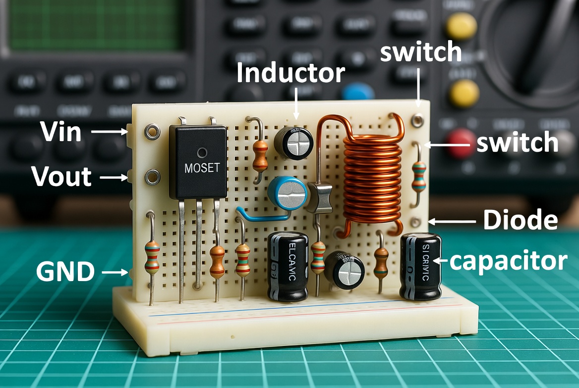
2.1 Power Switch
Typically a MOSFET, it controls when energy is drawn from the input source.
2.2 Inductor
Acts as an energy storage element that smooths current flow and limits current ripple.
2.3 Freewheeling Path
- Diode in non-synchronous designs
- MOSFET in synchronous designs
Provides a current path when the main switch is OFF.
2.4 Output Capacitor
Filters voltage ripple and stabilizes the output.
2.5 Controller
Generates switching signals and regulates output voltage using feedback.
3. Switching Operation and Energy Transfer
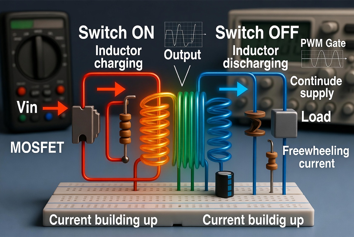
A buck converter operates in two repeating states:
3.1 Switch ON State
- Input voltage is applied across the inductor
- Inductor current increases linearly
- Energy is stored in the magnetic field
3.2 Switch OFF State
- Inductor releases stored energy
- Current flows through the diode or synchronous MOSFET
- Output voltage is maintained
This alternating process ensures continuous energy delivery to the load.
4. Operating Modes and Waveform Behavior
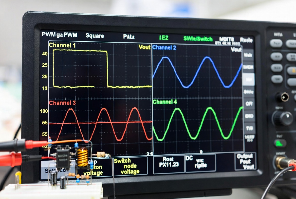
4.1 Continuous Conduction Mode CCM
- Inductor current never reaches zero
- Lower ripple and better efficiency
- Preferred for moderate to high load
4.2 Discontinuous Conduction Mode DCM
- Inductor current falls to zero each cycle
- Higher ripple and lower efficiency
- Occurs under light load conditions
4.3 Waveform Characteristics
- Switch voltage shows square waveform
- Inductor current shows triangular waveform
- Output voltage remains nearly constant with small ripple
5. Buck Converter Topologies
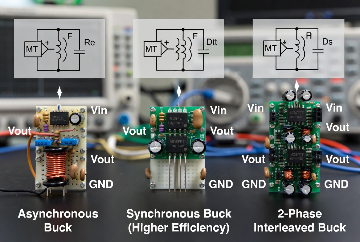
5.1 Non-Synchronous Buck
- Uses diode as freewheeling element
- Simpler and lower cost
- Efficiency limited by diode forward voltage
5.2 Synchronous Buck
- Replaces diode with MOSFET
- Lower conduction loss
- Higher efficiency, especially at high current
In modern designs, synchronous buck converters are preferred due to improved efficiency.
6. Practical Design Considerations
Designing a buck converter involves balancing electrical performance and physical constraints.
6.1 Duty Cycle
Determines output voltage ratio and influences switching stress.
6.2 Inductor Selection
- Larger inductance reduces ripple
- Smaller inductance improves transient response
6.3 Capacitor Selection
- Low ESR reduces voltage ripple
- Adequate capacitance improves stability
6.4 Switching Frequency
- Higher frequency reduces component size
- Increases switching losses
6.5 Thermal Design
Heat dissipation must be managed through layout and component choice.
7. Efficiency and Loss Mechanisms
No practical converter is lossless. Key loss contributors include:
7.1 MOSFET Losses
- Conduction loss (I^2 R)
- Switching loss during transitions
7.2 Diode Losses
- Forward voltage drop
- Reverse recovery losses
7.3 Inductor Losses
- Copper loss due to winding resistance
- Core loss due to magnetic hysteresis
7.4 Capacitor Losses
- ESR-related power dissipation
7.5 Layout Losses
- Parasitic inductance and resistance increase noise and loss
Optimization often involves trade-offs between efficiency, size, and cost.
8. Advantages and Limitations
Advantages
- High efficiency (often above 90%)
- Compact and scalable
- Suitable for a wide range of loads
Limitations
- Only reduces voltage
- Generates switching noise
- Requires careful PCB layout and filtering
9. Real World Applications
Buck converters are found in nearly every modern electronic system:
- Power supplies and adapters
- Mobile devices and battery-powered systems
- Automotive electronics
- Industrial control systems
- Telecommunications infrastructure
- Renewable energy systems
They are especially important wherever efficient voltage regulation is required.
10. Conclusion
The buck converter is a fundamental building block in power electronics. While the concept is simple, real performance depends on detailed design decisions involving switching behavior, component selection, and thermal management. Understanding these practical aspects is essential for building efficient and reliable power systems.
FAQ
1. Why is a buck converter more efficient than a linear regulator
Because it uses switching instead of dissipating excess energy as heat.
2. What determines output voltage
Primarily the duty cycle, along with losses and control accuracy.
3. When does DCM occur
At light load when inductor current drops to zero.
4. Why use synchronous rectification
To reduce conduction losses and improve efficiency.
5. What is the biggest design challenge
Balancing efficiency, size, thermal performance, and electromagnetic noise.