


Understanding Drift and Diffusion Currents in Semiconductors: A Complete Guide
Semiconductors are the backbone of modern electronics, powering everything from smartphones to electric vehicles. At the heart of semiconductor operation lies a fundamental concept: how charge carriers move through the material. This movement occurs through two primary mechanisms—drift and diffusion currents. Understanding these processes is essential for anyone working with semiconductor devices, from students to experienced engineers.
Table of Contents
- What Are Drift and Diffusion Currents?
- The Physics Behind Drift Current
- Understanding Diffusion Current Fundamentals
- Key Differences Between Drift and Diffusion
- Mathematical Equations and Formulas
- Drift and Diffusion in P-N Junctions
- Factors Affecting Current Flow
- Role in Semiconductor Devices
- Practical Applications and Real-World Examples
- Common Misconceptions and FAQs
1. What Are Drift and Diffusion Currents?
In semiconductors, electric current flows through the movement of charge carriers—electrons and holes. These carriers move through two distinct mechanisms that work simultaneously but are driven by different forces.
Drift current occurs when an external electric field is applied across a semiconductor. The field exerts a force on charge carriers, causing them to move in a specific direction. Electrons drift toward the positive terminal, while holes drift toward the negative terminal. This is similar to how a river current pushes a boat downstream.
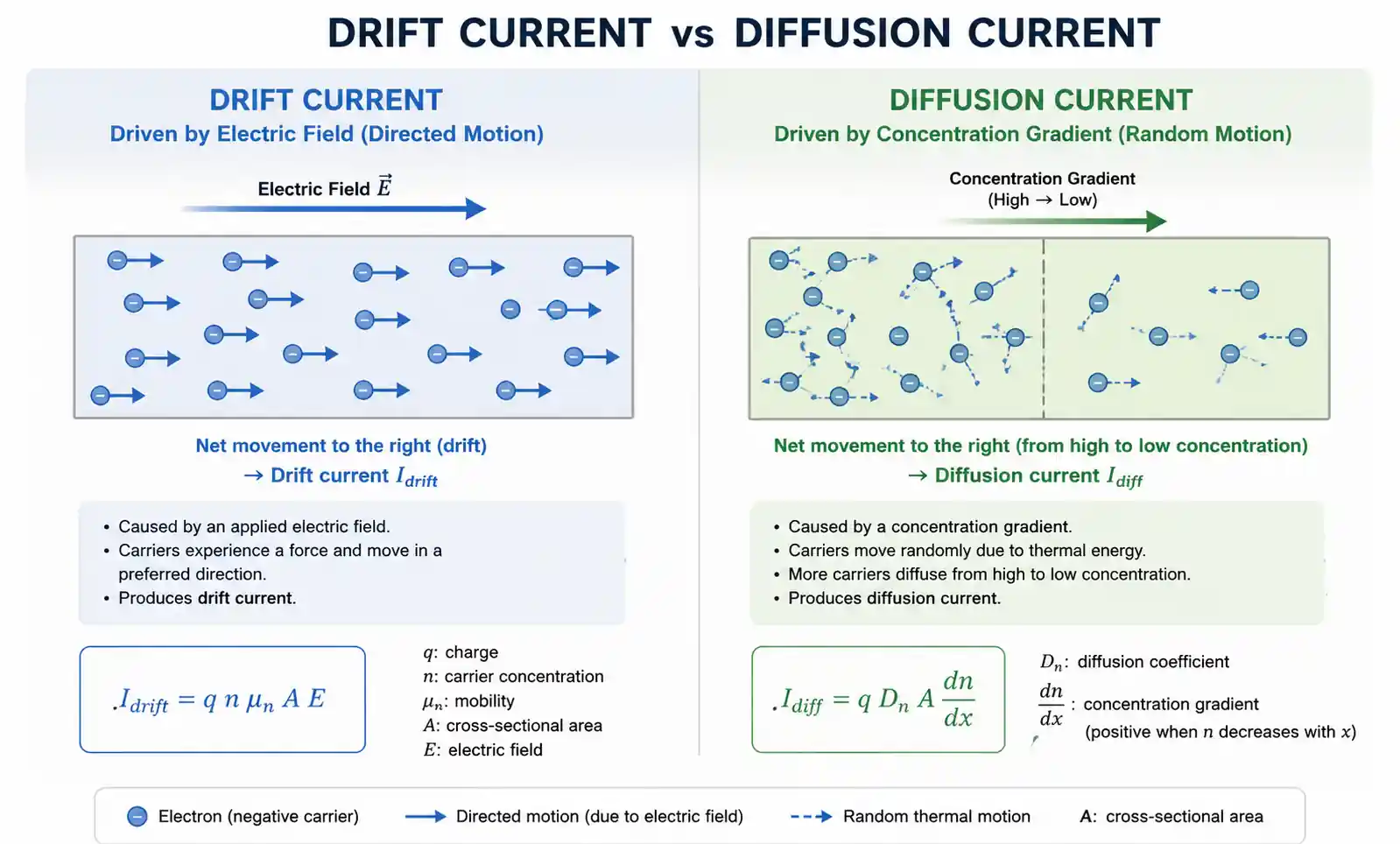
Diffusion current happens due to concentration gradients within the semiconductor material. When there's a higher concentration of carriers in one region compared to another, carriers naturally spread out from high-concentration areas to low-concentration areas. This process occurs even without an external electric field, driven purely by the random thermal motion of particles.
The total current in a semiconductor is the sum of both drift and diffusion components. In many devices, both mechanisms operate simultaneously, though one may dominate depending on the operating conditions.
2. The Physics Behind Drift Current
Drift current is fundamentally a response to an applied electric field. When you connect a voltage source across a semiconductor, it creates an electric field that permeates the material.
How Electric Fields Drive Carrier Motion
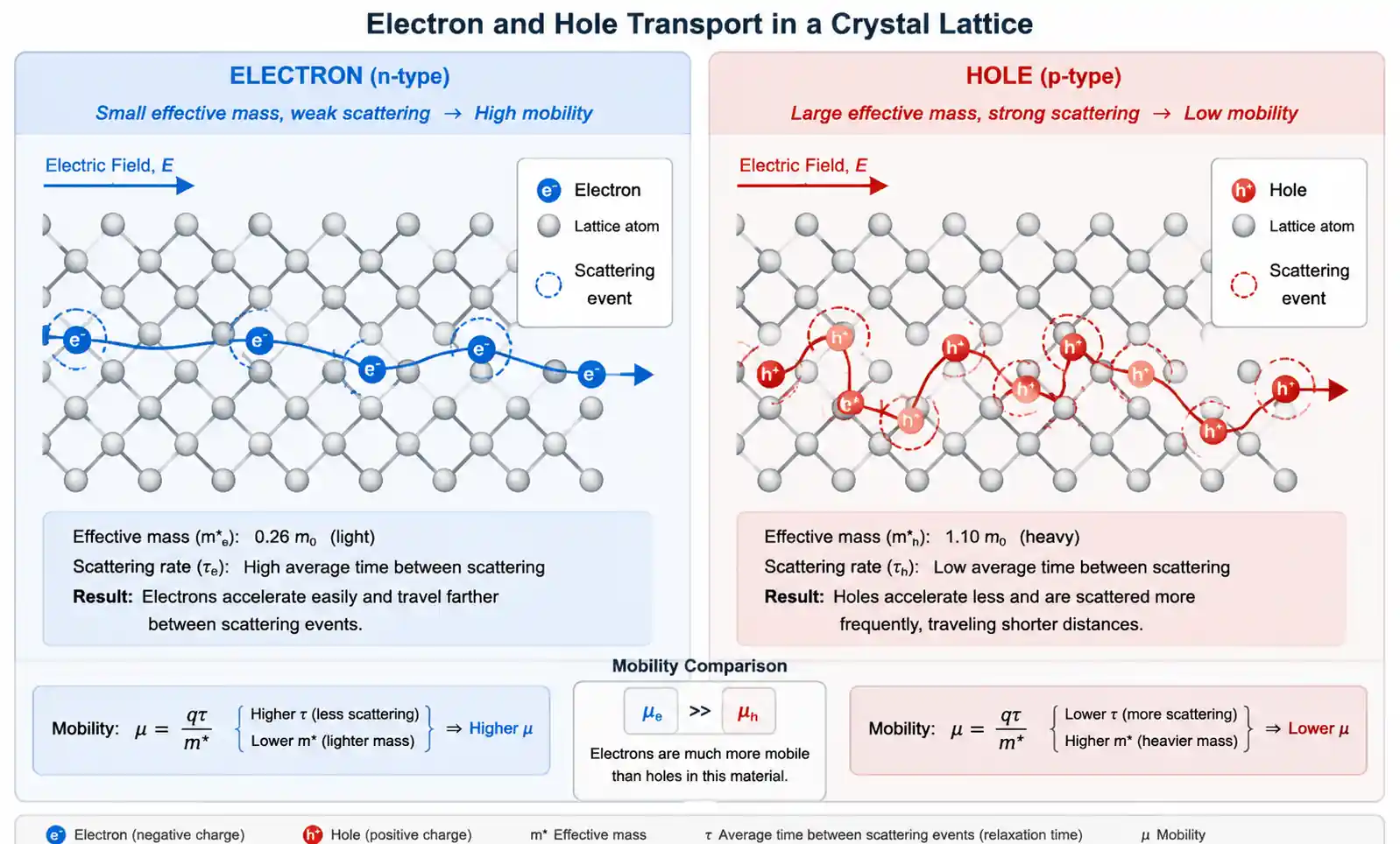
The electric field exerts a force on charge carriers according to the equation F = qE, where q is the charge and E is the electric field strength. Electrons, being negatively charged, experience a force opposite to the field direction. Holes, which represent the absence of electrons and behave as positive charges, move in the same direction as the field.
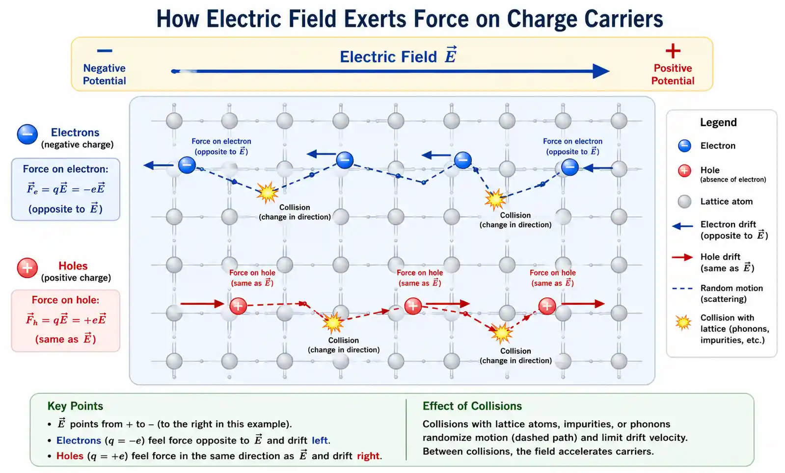
However, carriers don't accelerate indefinitely. As they move through the crystal lattice, they constantly collide with atoms, impurities, and other carriers. These collisions cause the carriers to lose momentum and change direction. The result is a net drift velocity in the direction of the applied field, rather than continuous acceleration.
Mobility and Drift Velocity
The average velocity that carriers achieve under an electric field is called the drift velocity (v_d). This velocity is proportional to the electric field strength:
v_d = μE
where μ (mu) is the carrier mobility. Mobility measures how easily carriers move through the semiconductor material. It depends on the material's crystal structure, temperature, and doping concentration.
Silicon, for example, has electron mobility around 1400 cm²/(V·s) and hole mobility around 450 cm²/(V·s) at room temperature. This means electrons move about three times faster than holes under the same electric field.
Temperature Effects on Drift
Temperature significantly impacts drift current. At higher temperatures, the crystal lattice vibrates more vigorously, increasing the frequency of carrier collisions. This reduces mobility and, consequently, drift velocity. This is why semiconductor devices often have temperature-dependent performance characteristics.
3. Understanding Diffusion Current Fundamentals
Diffusion is a natural process that occurs in many physical systems, from perfume spreading through a room to sugar dissolving in water. In semiconductors, diffusion drives carrier movement from regions of high concentration to regions of low concentration.
The Concentration Gradient
A concentration gradient exists whenever the carrier density varies across different regions of the semiconductor. This gradient is the driving force for diffusion current. The steeper the gradient, the stronger the diffusion current.
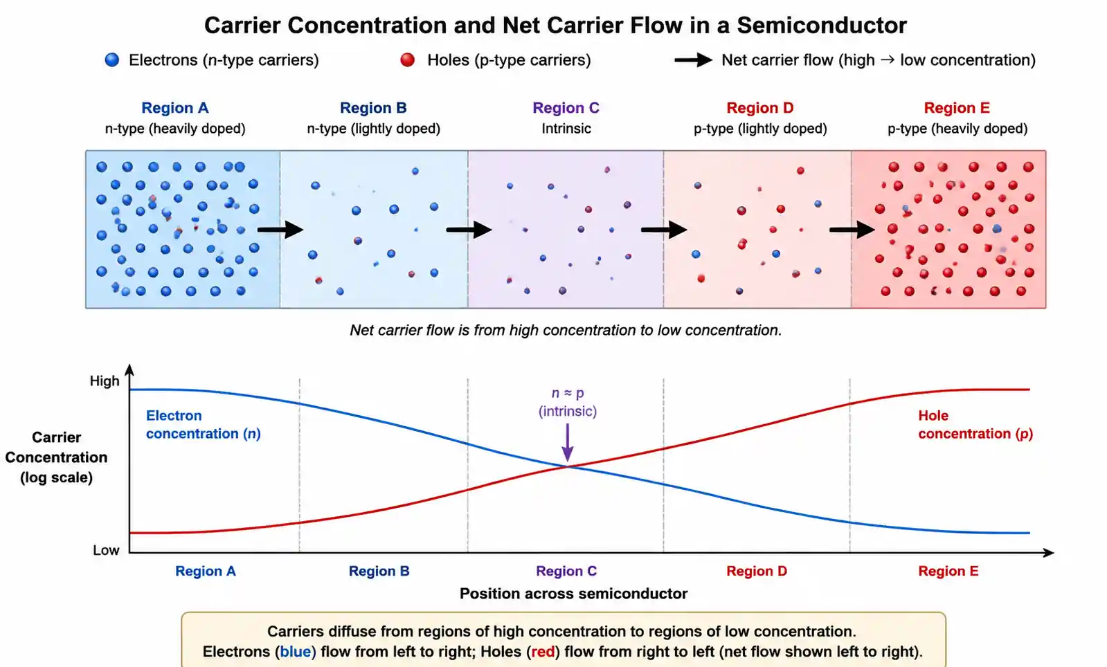
Consider a semiconductor where one region has been heavily doped with donor atoms (creating many free electrons) while an adjacent region has fewer carriers. The electrons in the high-concentration region undergo random thermal motion. Statistically, more electrons will move from the crowded region to the less crowded region than vice versa, creating a net flow of charge.
Random Thermal Motion
At any temperature above absolute zero, carriers possess thermal energy that causes them to move randomly through the crystal lattice. This motion is called Brownian motion or thermal diffusion. The average thermal velocity of carriers at room temperature is extremely high—around 10^7 cm/s—but the motion is random, so there's no net current unless a concentration gradient exists.
Fick's Law of Diffusion
The diffusion process in semiconductors follows Fick's first law, which states that the diffusion flux is proportional to the concentration gradient. For electrons:
J_n(diffusion) = qD_n(dn/dx)
where D_n is the electron diffusion coefficient, and dn/dx is the concentration gradient. The positive sign indicates that electrons flow from high to low concentration.
Diffusion Without External Fields
A key characteristic of diffusion current is that it occurs spontaneously without any external voltage or electric field. This makes it particularly important in devices like solar cells and photodiodes, where light creates localized carrier concentrations that then diffuse through the material.
4. Key Differences Between Drift and Diffusion
While both drift and diffusion contribute to current flow in semiconductors, they operate through fundamentally different mechanisms. Understanding these differences is crucial for analyzing semiconductor device behavior.
Driving Force
- Drift: Driven by an external electric field applied across the semiconductor
- Diffusion: Driven by concentration gradients within the material
Carrier Movement Direction
- Drift: Carriers move in the direction determined by the electric field (electrons opposite to field, holes along field)
- Diffusion: Carriers move from high-concentration regions to low-concentration regions, regardless of field direction
Dependence on External Voltage
- Drift: Directly proportional to applied voltage (higher voltage = stronger field = more drift current)
- Diffusion: Independent of external voltage; depends only on concentration gradients
Velocity Characteristics
- Drift: Produces a net directed velocity (drift velocity) superimposed on random thermal motion
- Diffusion: Results from random thermal motion with no preferred direction, but statistical bias toward lower concentration
Temperature Dependence
- Drift: Mobility decreases with temperature, reducing drift current
- Diffusion: Diffusion coefficient increases with temperature, enhancing diffusion current
Dominant Regions
- Drift: Dominates in neutral regions of semiconductors where electric fields are present
- Diffusion: Dominates in regions with steep concentration gradients, such as near junctions
5. Mathematical Equations and Formulas
The mathematical description of drift and diffusion currents provides quantitative tools for device design and analysis.
Drift Current Equations
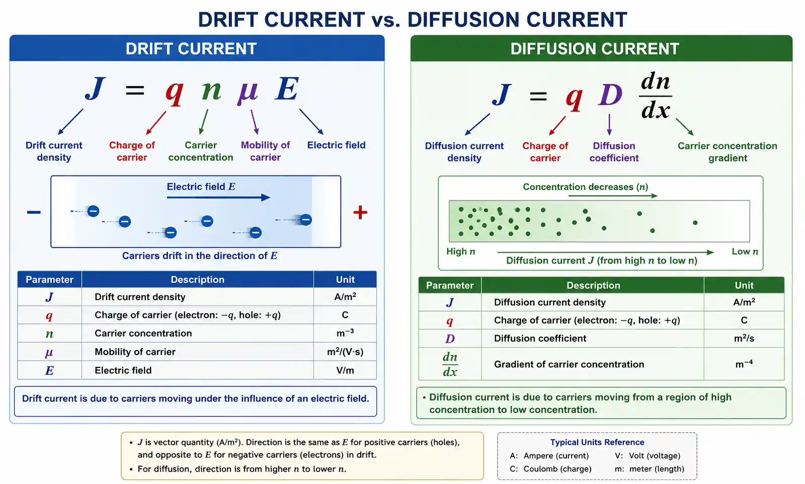
For electrons: J_n(drift) = qnμ_nE
For holes: J_p(drift) = qpμ_pE
where:
- J is current density (A/cm²)
- q is elementary charge (1.6 × 10^-19 C)
- n is electron concentration (cm^-3)
- p is hole concentration (cm^-3)
- μ_n is electron mobility (cm²/V·s)
- μ_p is hole mobility (cm²/V·s)
- E is electric field (V/cm)
Diffusion Current Equations
For electrons: J_n(diffusion) = qD_n(dn/dx)
For holes: J_p(diffusion) = -qD_p(dp/dx)
where:
- D_n is electron diffusion coefficient (cm²/s)
- D_p is hole diffusion coefficient (cm²/s)
- dn/dx and dp/dx are concentration gradients
Note the negative sign for holes: holes diffuse from high to low concentration, but since they carry positive charge, the current direction is opposite to the concentration gradient direction.
Einstein Relation
The diffusion coefficient and mobility are related through the Einstein relation:
D/μ = kT/q = V_T
where:
- k is Boltzmann's constant (1.38 × 10^-23 J/K)
- T is absolute temperature (K)
- V_T is thermal voltage (≈26 mV at room temperature)
This relation shows that materials with high mobility also have high diffusion coefficients.
Total Current Density
The total current density in a semiconductor is the sum of all components:
J_total = J_n(drift) + J_n(diffusion) + J_p(drift) + J_p(diffusion)
This equation is fundamental to semiconductor device modeling and appears in the drift-diffusion equations used in device simulators.
6. Drift and Diffusion in P-N Junctions
The p-n junction is the most fundamental semiconductor structure, and it beautifully demonstrates the interplay between drift and diffusion currents.
Junction Formation and Built-in Field
When p-type and n-type semiconductors are joined, a fascinating process occurs. The n-side has abundant free electrons, while the p-side has abundant holes. At the junction interface, electrons from the n-side diffuse into the p-side, and holes from the p-side diffuse into the n-side.
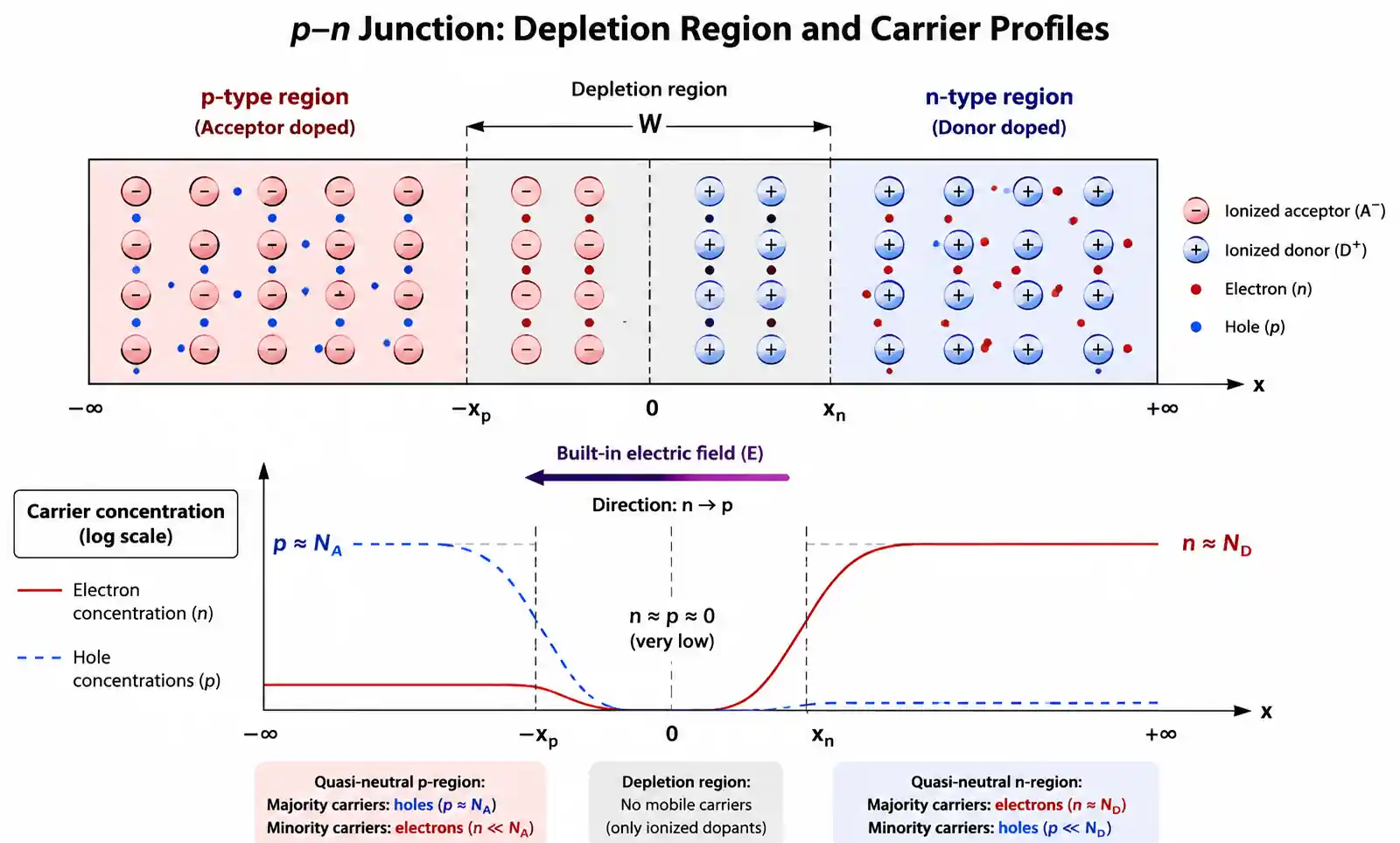
This diffusion leaves behind ionized dopant atoms—positive ions on the n-side and negative ions on the p-side. These immobile charges create a depletion region (also called space charge region) where mobile carriers are depleted. The ionized atoms generate an electric field pointing from the n-side to the p-side.
Equilibrium Condition
At thermal equilibrium (no external voltage), the built-in electric field creates a drift current that exactly balances the diffusion current. Electrons trying to diffuse from n to p are pushed back by the electric field. Similarly, holes trying to diffuse from p to n are pushed back. The result is zero net current:
J_drift + J_diffusion = 0
This equilibrium is maintained by the built-in potential (V_bi), typically 0.6-0.7V for silicon p-n junctions.
Forward Bias Operation
When a forward bias voltage is applied (positive to p-side, negative to n-side), it reduces the built-in electric field. The barrier for carrier diffusion decreases, allowing more carriers to diffuse across the junction. Diffusion current dominates, and substantial current flows through the device.
Reverse Bias Operation
Under reverse bias (negative to p-side, positive to n-side), the electric field strengthens. The barrier increases, nearly eliminating diffusion current. Only a small drift current flows, carried by minority carriers generated by thermal processes. This is the reverse saturation current.
Depletion Region Dynamics
The width of the depletion region changes with applied voltage. Forward bias narrows it, while reverse bias widens it. This voltage-dependent capacitance is exploited in varactor diodes used for voltage-controlled tuning in RF circuits.
7. Factors Affecting Current Flow
Several factors influence the magnitude and behavior of drift and diffusion currents in semiconductors.
Doping Concentration
Doping introduces impurity atoms that dramatically alter carrier concentrations. Heavy doping increases the number of majority carriers, enhancing drift current capability. However, it also reduces mobility due to increased impurity scattering, creating a trade-off in device design.
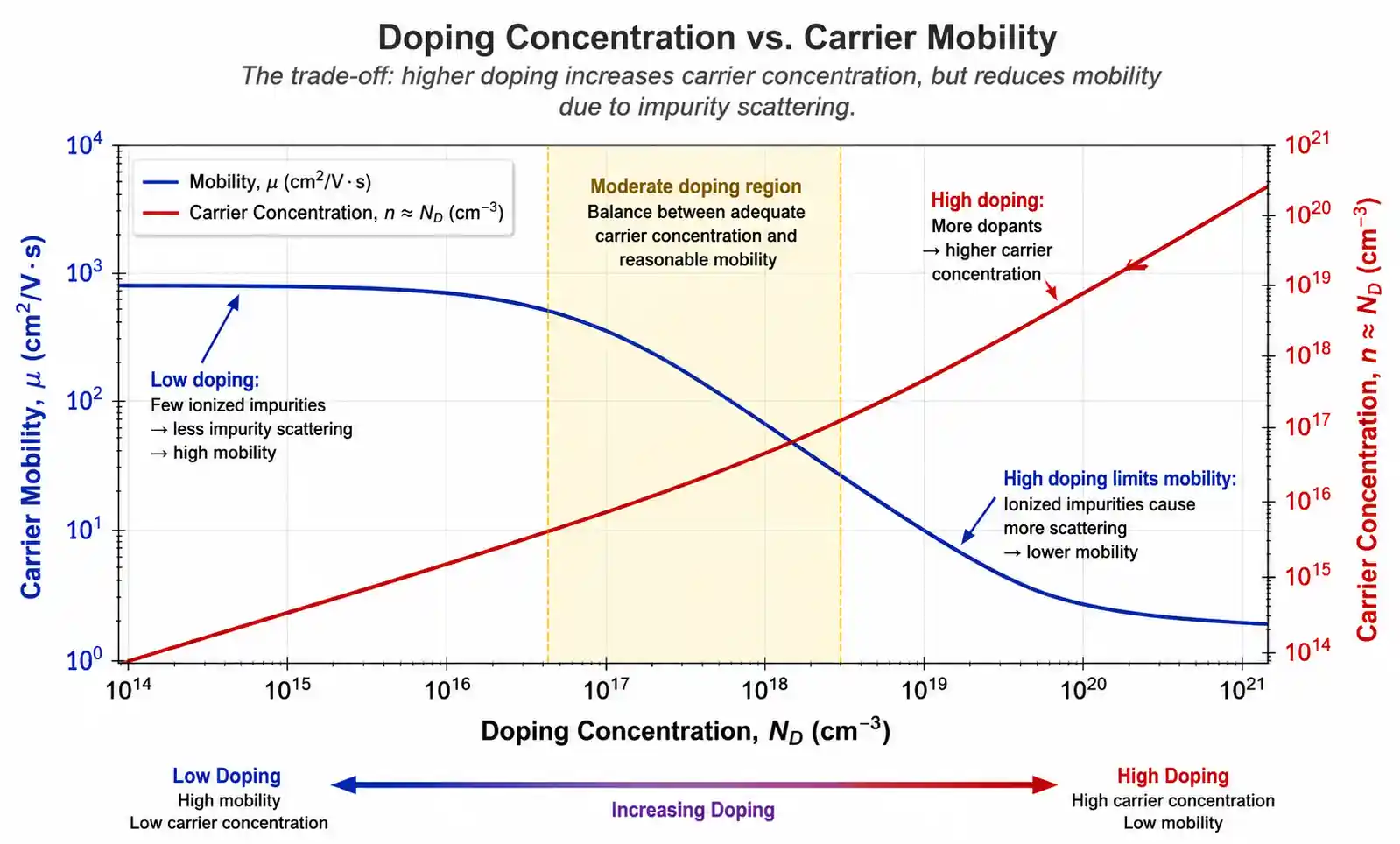
In diffusion-dominated regions, doping creates the concentration gradients that drive diffusion current. The steeper the doping profile, the stronger the diffusion current.
Temperature Effects
Temperature has complex effects on semiconductor behavior:
On drift current: Higher temperature increases lattice vibrations, reducing mobility and drift current. This is why semiconductor resistivity increases with temperature.
On diffusion current: Higher temperature increases thermal energy, enhancing diffusion coefficients and diffusion current. The Einstein relation shows this explicitly through the kT term.
On carrier concentration: Temperature increases intrinsic carrier concentration exponentially, affecting both drift and diffusion in lightly doped regions.
Electric Field Strength
The electric field directly controls drift current through the relationship J = qnμE. However, at very high fields (>10^4 V/cm in silicon), carrier velocity saturates due to increased scattering. This velocity saturation limits the performance of short-channel transistors.
Material Properties
Different semiconductor materials have vastly different transport properties:
- Silicon: Moderate mobility, excellent for integrated circuits
- Gallium Arsenide (GaAs): High electron mobility, used in high-frequency devices
- Silicon Carbide (SiC): Wide bandgap, excellent for high-temperature and high-power applications
- Gallium Nitride (GaN): Very high electron mobility, used in power electronics and LEDs
Crystal Quality and Defects
Crystal defects, grain boundaries, and impurities create scattering centers that reduce mobility. High-quality single-crystal materials are essential for high-performance devices. This is why semiconductor manufacturing requires ultra-clean environments and precise crystal growth techniques.
8. Role in Semiconductor Devices
Drift and diffusion currents are not just theoretical concepts—they determine how every semiconductor device operates.
Bipolar Junction Transistors (BJTs)
In BJTs, both mechanisms are critical. When the base-emitter junction is forward biased, minority carriers (electrons in a PNP or holes in an NPN) are injected into the base region. These carriers diffuse across the narrow base region toward the collector. The diffusion current through the base is the primary mechanism of transistor action.
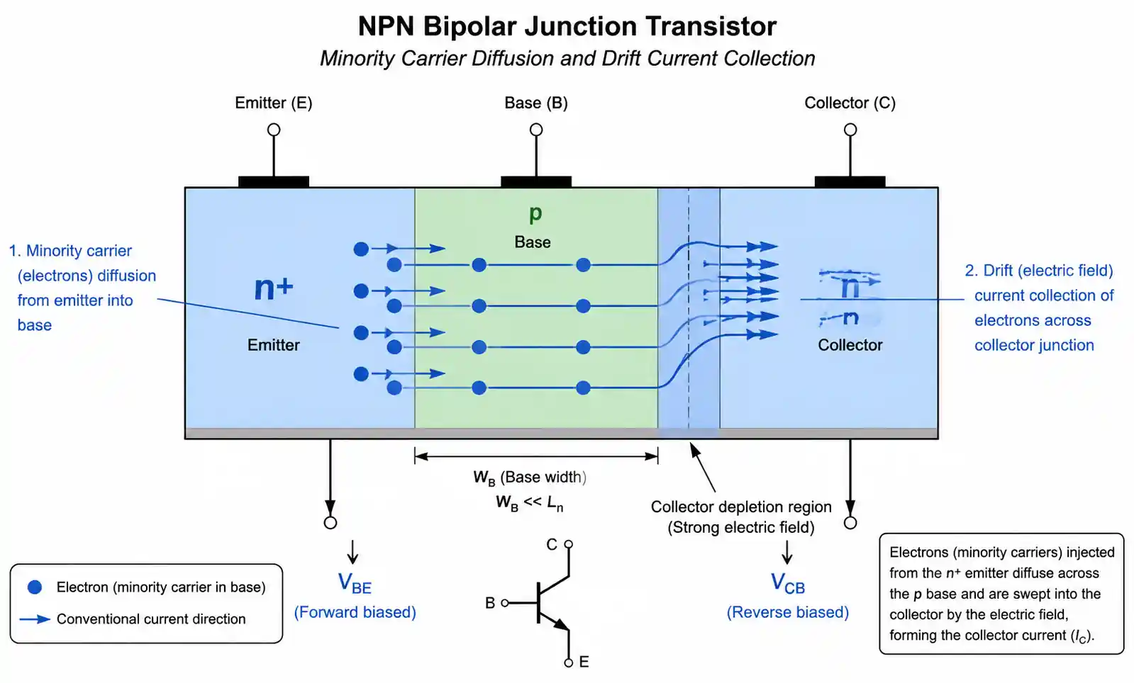
Meanwhile, drift current flows in response to the collector-base electric field, sweeping carriers into the collector. The transistor's current gain depends on the balance between diffusion across the base and recombination within it.
MOSFETs (Metal-Oxide-Semiconductor Field-Effect Transistors)
In MOSFETs, drift current dominates. When a gate voltage creates an inversion layer (channel) at the semiconductor-oxide interface, carriers drift from source to drain under the influence of the drain-source voltage. The channel conductivity depends on carrier mobility and the electric field strength.
Modern short-channel MOSFETs operate in the velocity saturation regime, where drift velocity reaches its maximum value regardless of further field increases. This limits the performance scaling of transistors.
Solar Cells and Photodiodes
These devices rely heavily on diffusion. When light generates electron-hole pairs in the semiconductor, these carriers diffuse toward the p-n junction. The built-in electric field then separates them, creating photocurrent. The diffusion length—how far carriers can diffuse before recombining—is a critical parameter determining device efficiency.
Light-Emitting Diodes (LEDs)
In LEDs, forward bias causes electrons and holes to diffuse toward the junction from opposite sides. When they meet in the active region, they recombine, releasing energy as photons. The efficiency depends on how effectively carriers diffuse to the recombination zone and the radiative recombination rate.
Power Devices
High-voltage power devices like IGBTs (Insulated Gate Bipolar Transistors) and power MOSFETs must handle large currents and voltages. Their design carefully balances drift and diffusion to minimize power loss while maintaining fast switching speeds. The drift region must be thick enough to support high voltages but not so thick that it creates excessive resistance.
9. Practical Applications and Real-World Examples
Understanding drift and diffusion currents has direct implications for modern technology.
Integrated Circuit Design
Modern microprocessors contain billions of transistors, each relying on precise control of drift and diffusion. Circuit designers must account for:
- Short-channel effects: As transistors shrink, diffusion from source and drain regions affects channel behavior
- Leakage currents: Unwanted diffusion and drift currents that waste power
- Temperature management: Drift and diffusion respond differently to temperature, affecting circuit reliability
Sensor Technology
Many sensors exploit drift and diffusion mechanisms:
- Temperature sensors: Use the temperature dependence of drift and diffusion
- Pressure sensors: Piezoresistive sensors rely on stress-induced changes in carrier mobility
- Chemical sensors: Detect gases by measuring changes in surface carrier concentrations
Renewable Energy
Solar cell efficiency depends critically on minority carrier diffusion length. Longer diffusion lengths mean carriers generated deep in the material can reach the junction before recombining, improving efficiency. Modern high-efficiency solar cells use:
- Passivation layers: Reduce surface recombination, extending effective diffusion length
- Back-surface fields: Create drift fields that reflect minority carriers back toward the junction
- Textured surfaces: Increase light absorption and carrier generation
Power Electronics
Electric vehicles, renewable energy systems, and industrial motor drives all depend on power semiconductor devices. These devices must efficiently switch large currents and voltages. Engineers optimize:
- Drift region design: Balance voltage blocking capability with on-resistance
- Carrier lifetime control: Adjust recombination rates to optimize switching speed
- Temperature management: Account for temperature effects on drift and diffusion
Emerging Technologies
New applications continue to emerge:
- Quantum computing: Requires precise control of carrier behavior at nanoscale
- Neuromorphic computing: Mimics biological neurons using drift-diffusion dynamics
- Flexible electronics: Must maintain carrier transport in mechanically stressed materials
10. Common Misconceptions and FAQs
Does diffusion current require a voltage?
No. Diffusion current is driven by concentration gradients, not voltage. It occurs spontaneously whenever carrier concentration varies spatially, even with no external voltage applied. This is fundamentally different from drift current, which requires an electric field.
Can drift and diffusion currents flow in opposite directions?
Yes, absolutely. In a forward-biased p-n junction, for example, diffusion current flows from p to n (for holes) while the electric field would cause drift in the opposite direction. The net current is the sum of both components.
Why do electrons and holes have different mobilities?
Electrons and holes interact differently with the crystal lattice. Electrons have lower effective mass and scatter less frequently, giving them higher mobility. Holes, being the absence of electrons in the valence band, have higher effective mass and lower mobility. The exact values depend on the semiconductor material and crystal structure.
What happens to drift and diffusion at very low temperatures?
At very low temperatures, carrier mobility increases dramatically because lattice vibrations decrease. However, carrier concentration also drops exponentially in intrinsic and lightly doped semiconductors. The net effect depends on the specific device and doping levels. Some devices, like superconducting electronics, exploit near-zero temperature operation.
How do drift and diffusion relate to Ohm's Law?
In uniform semiconductors with only drift current, the relationship J = σE (where σ is conductivity) is Ohm's Law. However, when diffusion is significant, the simple Ohmic relationship breaks down. The full drift-diffusion equations must be used, which include both drift and diffusion terms.
Can we have pure drift or pure diffusion in real devices?
In practice, both mechanisms almost always coexist. However, one often dominates:
- Pure drift approximation: Valid in long, uniformly doped resistors with applied voltage
- Pure diffusion approximation: Valid in regions with steep concentration gradients and weak electric fields, such as the neutral base region of a BJT
How does device scaling affect drift and diffusion?
As devices shrink to nanometer scales, several effects emerge:
- Electric fields become extremely high, causing velocity saturation
- Diffusion becomes more significant relative to drift in short channels
- Quantum effects begin to influence carrier transport
- Short-channel effects cause unwanted diffusion from source and drain
These challenges drive ongoing research in semiconductor device physics and novel device architectures.
Conclusion
Drift and diffusion currents are the fundamental mechanisms of charge transport in semiconductors. Drift, driven by electric fields, provides controlled carrier movement in response to applied voltages. Diffusion, driven by concentration gradients, enables spontaneous carrier redistribution that is essential for junction operation.
Every semiconductor device—from the simplest diode to the most complex microprocessor—relies on the interplay between these two mechanisms. Understanding their physics, mathematics, and practical implications is essential for anyone working in electronics, whether designing circuits, developing new materials, or troubleshooting device behavior.
As semiconductor technology continues to advance toward smaller dimensions, higher speeds, and new materials, the fundamental principles of drift and diffusion remain as relevant as ever. They provide the foundation for innovation in computing, communications, energy, and countless other applications that define modern technology.