



EMI/EMC Design Guide for Electronic Component Selection
Electromagnetic interference (EMI) causes over 30% of failed compliance tests in power electronics and industrial control systems, resulting in costly redesigns averaging $50,000 to $200,000 per iteration. For design engineers, selecting the right filtering components, understanding their electrical behavior, and implementing proper PCB layout practices prevents EMI/EMC failures before prototype fabrication. This guide provides component selection criteria, filter topology analysis, and layout techniques validated through emissions testing.
At Hitop Tech Limited, our procurement services support engineers with sourcing EMI/EMC compliant components backed by manufacturer test data and certification documentation.
Table of Contents
- Understanding EMI Sources and Regulatory Standards
- Filter Component Selection: Capacitors and Inductors
- Common-Mode vs Differential-Mode Filtering Strategies
- Filter Topology Design: L, Pi, and T Configurations
- PCB Layout Impact on EMI Performance
- Component Specifications for Compliance Testing
- FAQ
- Conclusion
1. Understanding EMI Sources and Regulatory Standards
EMI originates from switching transients in power converters, clock harmonics in digital circuits, and inductive load commutation. Understanding these mechanisms guides component selection for effective suppression. Conducted emissions propagate through power lines and cables (150 kHz to 30 MHz), while radiated emissions couple through electromagnetic fields (30 MHz to 1 GHz).
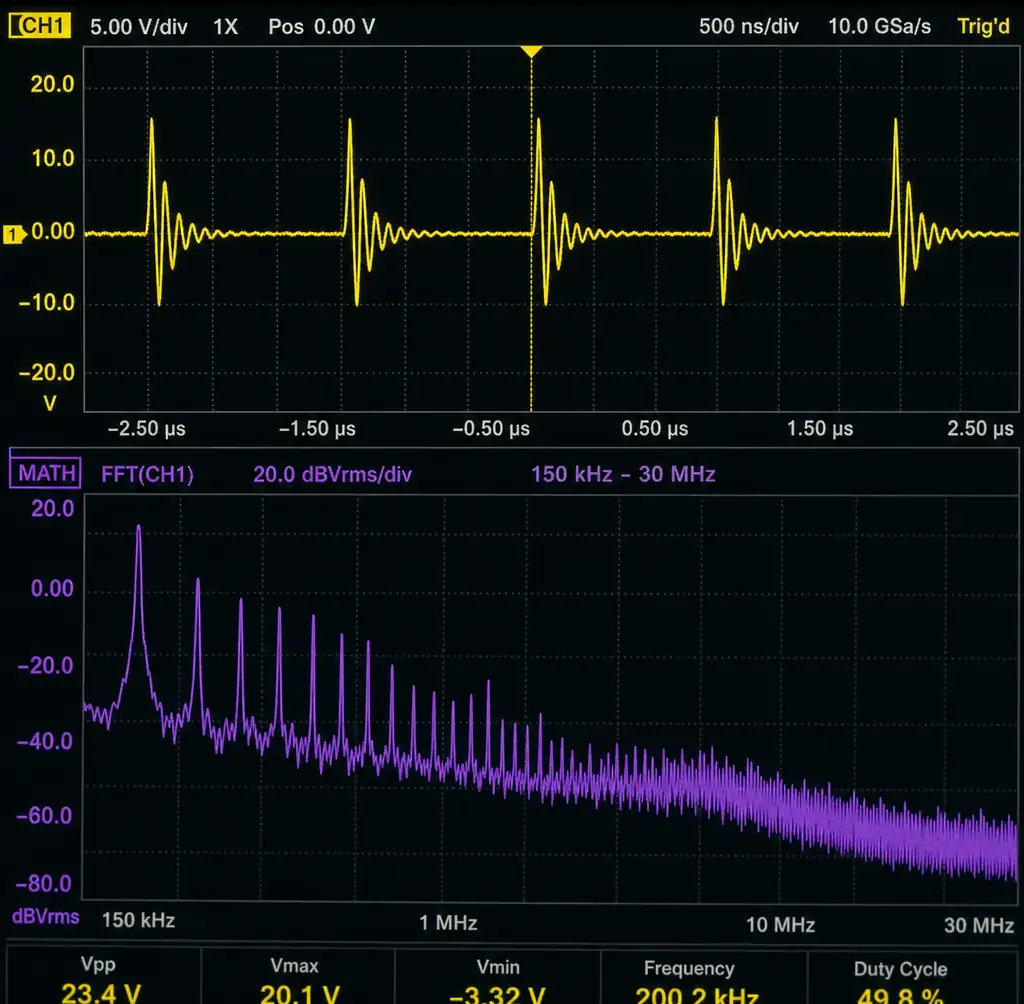 Oscilloscope measurement showing switching transient EMI noise waveform with frequency spectrum
Regulatory compliance requirements vary by application and region. Industrial equipment follows IEC 61000-6-4 (Class A limits, 10 dB more relaxed than residential), while consumer electronics must meet FCC Part 15B or EN 55032 (Class B limits). Automotive systems operate under CISPR 25 with specific limits for different frequency bands. Medical devices face the strictest requirements under IEC 60601-1-2 with immunity testing mandatory.
| Standard | Application | Conducted Emissions | Radiated Emissions | Key Requirement |
|---|---|---|---|---|
| FCC Part 15B Class B | Consumer electronics | 0.15-30 MHz: 46-56 dBμV | 30-1000 MHz: 40-46 dBμV/m @ 3m | Residential use compliance |
| EN 55032 Class A | Industrial equipment | 0.15-30 MHz: 66-76 dBμV | 30-1000 MHz: 50 dBμV/m @ 10m | Industrial environment tolerance |
| CISPR 25 Class 5 | Automotive systems | 0.15-108 MHz: 36-60 dBμV | 150 kHz-2.5 GHz: variable limits | Vehicle EMC environment |
| IEC 60601-1-2 | Medical devices | EN 55011 limits + margins | 80 MHz-2.7 GHz: 3-10 V/m immunity | Patient safety critical |
Testing costs drive design-for-EMC approaches. Pre-compliance testing using near-field probes costs $500-2,000 internally, while full compliance testing at accredited labs runs $8,000-15,000 per iteration. Each redesign adds 4-8 weeks to development timelines. Component selection errors—wrong capacitor type, insufficient inductance, missing common-mode suppression—account for 60% of initial test failures.
2. Filter Component Selection: Capacitors and Inductors
EMI filter performance depends critically on component parasitics. At high frequencies, real capacitors exhibit series inductance (ESL) and equivalent series resistance (ESR), while inductors show parasitic capacitance. Selecting components with favorable high-frequency characteristics ensures filter effectiveness across the entire compliance frequency range.
Capacitor Selection for EMI Suppression
X-capacitors (line-to-line) suppress differential-mode noise, while Y-capacitors (line-to-ground) attenuate common-mode currents. Film capacitors—polyester (X1/X2) and polypropylene (X1)—offer low ESL (5-20 nH) and self-healing properties critical for safety. For X-capacitors, select X2-rated (2.5 kV surge) for 230 VAC applications and X1-rated (4.0 kV surge) for industrial 400 VAC systems.
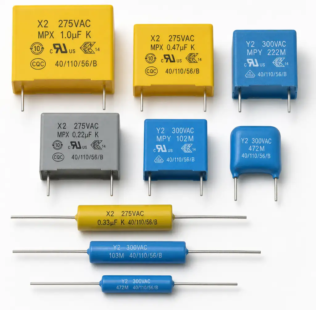 X-rated and Y-rated safety capacitors showing physical construction and markings
Y-capacitors connect live conductors to protective earth, creating leakage current. Safety standards limit this to 0.25-3.5 mA depending on equipment class. Y2-rated capacitors (5 kV surge) suit Class I equipment with protective earth, while Y1-rated (8 kV surge) handle basic insulation applications. Typical values range 1-10 nF to balance filtering effectiveness against leakage current limits.
Ceramic capacitors provide high-frequency suppression (10 MHz-1 GHz) due to ultra-low ESL (0.5-2 nH in 0805 packages). However, Class II dielectrics (X5R, X7R) exhibit voltage and temperature derating—a 10 μF/25V X7R capacitor loses 60% capacitance at rated voltage and 15% at temperature extremes. For critical filtering, verify actual capacitance under operating conditions.
| Capacitor Type | Frequency Range | Typical ESL | Application | Key Limitation |
|---|---|---|---|---|
| X2 film (line-to-line) | 150 kHz-10 MHz | 15-40 nH | DM noise suppression | Physical size at high capacitance |
| Y2 film (line-to-ground) | 150 kHz-30 MHz | 20-50 nH | CM noise to ground | Leakage current limits (nF range) |
| MLCC X7R 0805 | 1-100 MHz | 0.8-1.5 nH | High-frequency bypass | Voltage/temp derating, microphonics |
| MLCC C0G 0603 | 10-500 MHz | 0.5-1.0 nH | Ultra-stable filtering | Low capacitance values only |
Inductor Selection for EMI Filtering
Common-mode chokes suppress noise present equally on both conductors without affecting differential signals. Effective permeability (μe) of 2,000-10,000 provides high impedance (1-10 kΩ) at frequencies above 1 MHz. Ferrite core materials—Mn-Zn for 150 kHz-10 MHz, Ni-Zn for 10-200 MHz—must match the target frequency range.
Differential-mode inductors carry full load current and require cores with low saturation flux density margins. Powdered iron cores (MPP, High Flux, Sendust) handle DC bias without core saturation. For a 5A application, select inductors rated 6-8A to maintain inductance under load—saturation reduces 100 μH to 20 μH, destroying filter effectiveness.
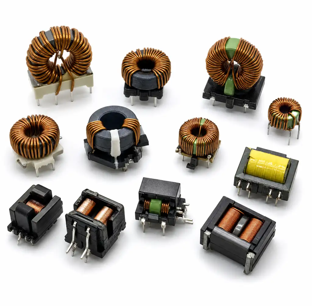 Common-mode choke inductors with different ferrite core materials and winding configurations
3. Common-Mode vs Differential-Mode Filtering Strategies
EMI noise contains both common-mode (CM) and differential-mode (DM) components requiring separate filtering strategies. Measurement with current probes distinguishes these modes—CM current flows in-phase on both conductors, while DM current flows in opposite directions. Effective filters address both modes across the full frequency spectrum.
Common-Mode Filtering
CM chokes present high impedance to in-phase currents while offering near-zero impedance to load current. A 2 mH CM choke with 2,000 permeability provides 12 kΩ impedance at 1 MHz, attenuating CM noise by 30-40 dB when paired with Y-capacitors. For three-phase systems, use three-winding CM chokes or delta-connected single-phase chokes.
CM choke effectiveness degrades above self-resonant frequency (SRF) due to interwinding capacitance (typically 10-50 pF). For broadband suppression, cascade two chokes optimized for different frequency ranges—one for 150 kHz-10 MHz using Mn-Zn ferrite, another for 10-100 MHz using Ni-Zn ferrite.
Differential-Mode Filtering
DM filters use series inductors and shunt capacitors forming LC or multi-stage networks. Cutoff frequency calculation follows: fc = 1/(2π√LC). For a 50 μH inductor with 1 μF capacitor, fc = 22.5 kHz. This provides approximately 40 dB/decade attenuation above cutoff, requiring 3-6x margin below the lowest target frequency for effective suppression.
| Parameter | Common-Mode Choke | Differential-Mode Inductor | Design Trade-off |
|---|---|---|---|
| Inductance per winding | 1-10 mH typical | 10-500 μH typical | CM: high Z needed; DM: limited by DCR |
| DC current rating | Full load current | Full load current | Core saturation vs size |
| Core material | High-μ ferrite (2K-10K) | Low-μ powdered (60-125) | CM: maximize μ; DM: avoid saturation |
| Parasitic capacitance | 10-50 pF (interwinding) | 5-20 pF (turn-to-turn) | Limits high-frequency performance |
| Insertion loss @ 1 MHz | 30-50 dB (with Y-caps) | 20-30 dB (with X-caps) | CM dominates conducted emissions |
4. Filter Topology Design: L, Pi, and T Configurations
Filter topology selection balances attenuation requirements, source/load impedance, and physical constraints. Single-stage L-filters provide 20 dB/decade rolloff, while multi-stage Pi and T networks achieve 40-60 dB/decade with proper impedance matching.
L-Section Filters
The simplest topology places series inductor and shunt capacitor. Source impedance affects performance significantly—low source impedance (switching converters: 0.1-1 Ω) requires capacitor-first CL configuration, while high source impedance (flyback converters: 10-100 Ω) needs inductor-first LC arrangement. Mismatch reduces attenuation by 10-20 dB.
Pi-Section Filters
Pi topology (C-L-C) provides symmetric impedance matching and second-order filtering (40 dB/decade). The first shunt capacitor matches source impedance, series inductor provides isolation, and second capacitor matches load impedance. For SMPS applications with 0.5 Ω source impedance and 50 Ω cable, typical values: C1 = 10 μF, L = 100 μH, C2 = 0.47 μF.
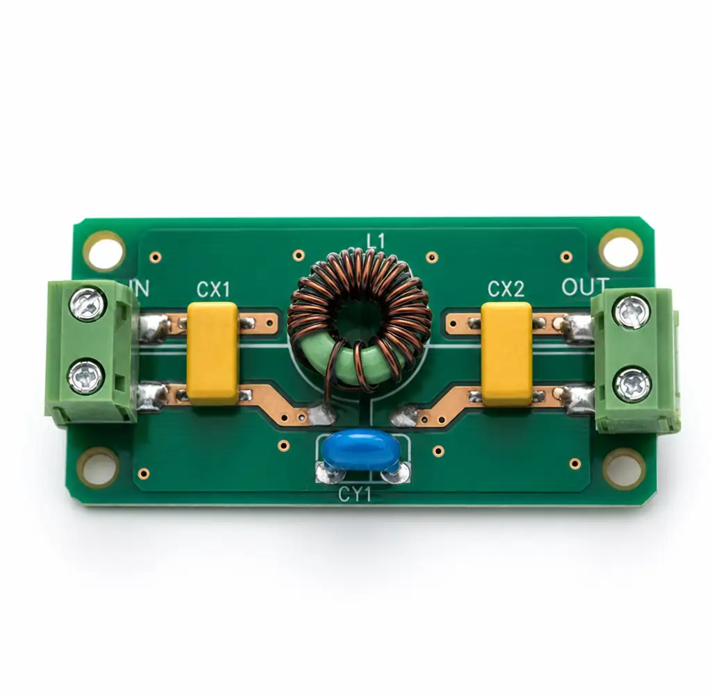 PCB layout showing Pi-section EMI filter component placement and trace routing
T-Section and Multi-Stage Designs
T topology (L-C-L) suits high source impedance applications. Industrial motor drives benefit from T-filters with 100 μH/1 μF/100 μH configurations providing 45 dB attenuation at 1 MHz. For challenging compliance cases, cascade two Pi-sections with damping resistors (5-10 Ω) between stages to prevent resonance amplification—undamped cascaded filters can increase emissions by 15-20 dB at resonance.
5. PCB Layout Impact on EMI Performance
Component selection alone cannot ensure EMI compliance—PCB layout creates parasitic inductance and coupling paths that degrade filter performance by 20-40 dB. Layout rules must be followed systematically from power entry through filtering stages to switching circuits.
Grounding and Return Path Management
Single-point grounding at filter input prevents ground loops. Connect filter ground to chassis earth through a single, wide trace (>5 mm). Never allow switching currents to share return paths with filter components—a 5A switching current through 10 nH trace inductance generates 50V transients at 1 MHz switching frequency.
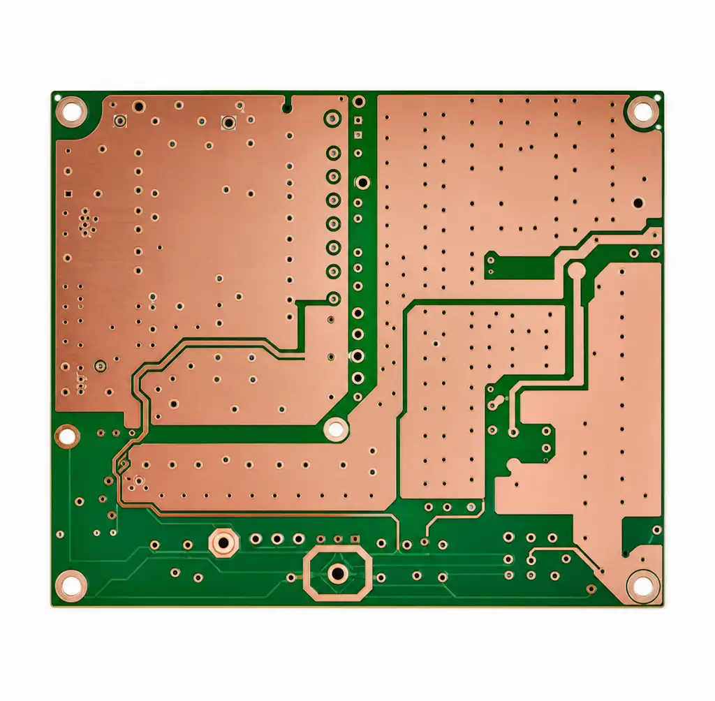 PCB ground plane layout showing separated power ground and signal ground zones
Create separate ground zones: PGND (power/switching), AGND (control/sensing), and EGND (earth/chassis). Connect these zones at one point only, typically at the power entry. Multi-point ground connections create loop antennas with radiation efficiency proportional to loop area.
Component Placement and Trace Routing
Place filter components within 25 mm of connector entry. Route power traces through filter components before reaching switching circuits—reverse routing allows noise to bypass the filter. Minimize loop area between X-capacitor connection points (<100 mm²) and Y-capacitor ground paths (<50 mm²).
Use ground pour between filter input and output stages as EMI barrier. Leave 3-5 mm guard gap between input and output traces to prevent capacitive coupling. A 1 pF parasitic coupling capacitance between input and output reduces filter effectiveness by 20 dB above 10 MHz.
| Layout Aspect | Recommended Practice | Impact of Non-Compliance | Verification Method |
|---|---|---|---|
| Filter-to-connector distance | <25 mm trace length | 10-15 dB loss per 50 mm | Measure with near-field probe |
| X-cap loop area | <100 mm² enclosed area | 6 dB loss per 2x area increase | Calculate from layout geometry |
| Y-cap to ground via | <10 mm, multiple vias | 15-20 dB loss above 30 MHz | TDR measurement of impedance |
| Input/output trace separation | >3 mm clearance, ground barrier | 20-30 dB crosstalk above 10 MHz | Two-port S21 measurement |
| Ground plane continuity | Unbroken reference under filter | 10-25 dB degradation if broken | Return current visualization |
6. Component Specifications for Compliance Testing
Datasheet parameters must align with actual operating conditions during compliance testing. Temperature, voltage bias, and frequency-dependent behaviors significantly affect real-world performance versus nominal specifications.
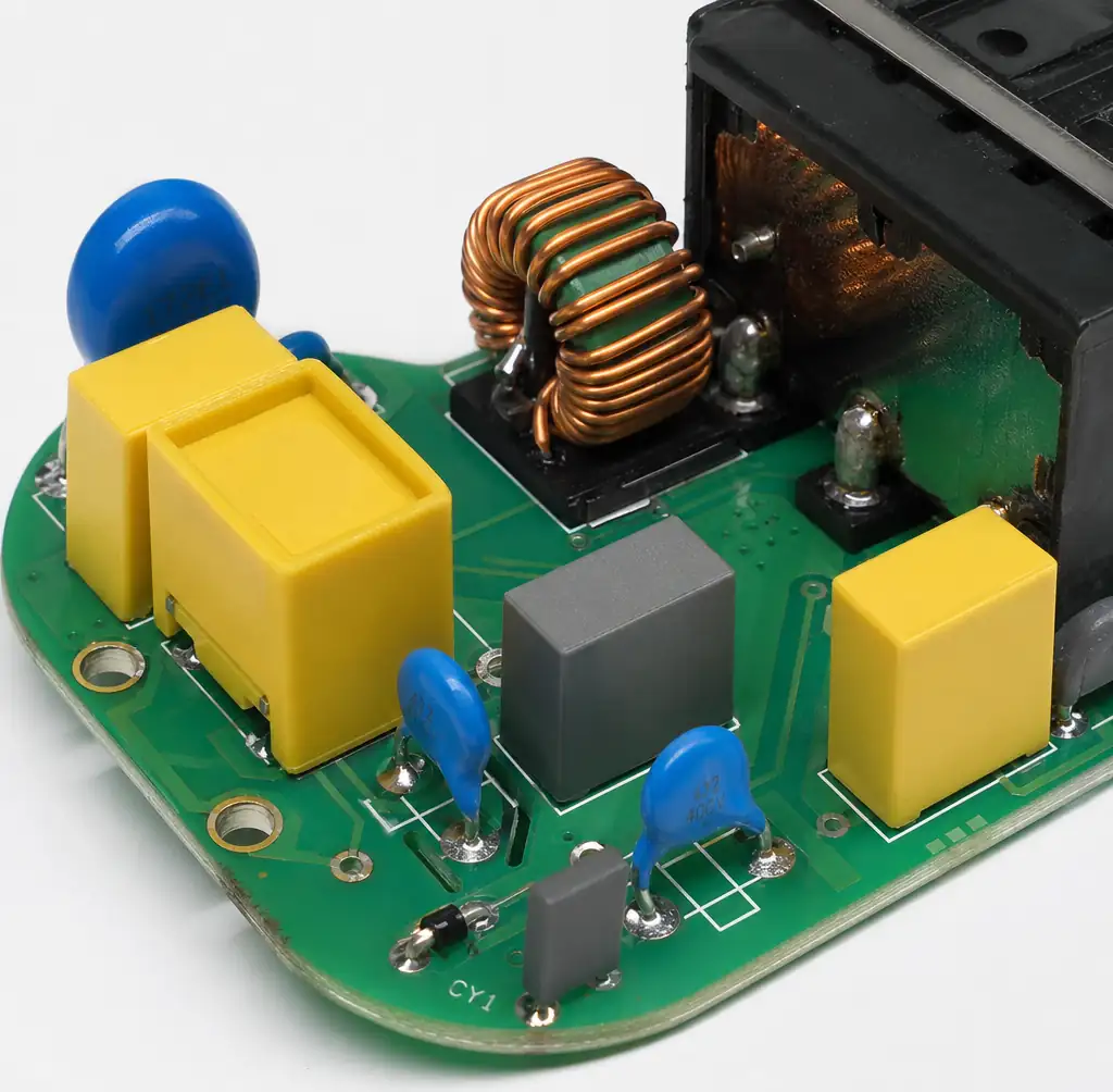 Close-up view of EMI filter components showing proper trace routing and spacing
Frequency-Dependent Impedance
Capacitor impedance follows |Z| = 1/(2πfC) only below self-resonant frequency. Above SRF, ESL dominates and impedance rises inductively. A 10 μF ceramic capacitor with 2 nH ESL resonates at 1.1 MHz—effective for 150 kHz to 1 MHz filtering but provides minimal suppression at 10 MHz.
Review manufacturer impedance vs frequency curves rather than relying on nominal capacitance. For broadband suppression (150 kHz to 100 MHz), parallel multiple capacitor values—10 μF for low frequencies, 0.1 μF for mid-range, 10 nF for high frequencies. Ensure low-inductance mounting with minimum via count and wide traces.
Current Rating and Thermal Management
AC ripple current in filter capacitors generates I²R heating in ESR. A 1 μF film capacitor with 50 mΩ ESR dissipates 0.5W at 3A RMS ripple current, raising temperature 30-50°C depending on thermal coupling. This accelerates aging and risks thermal runaway in compact layouts.
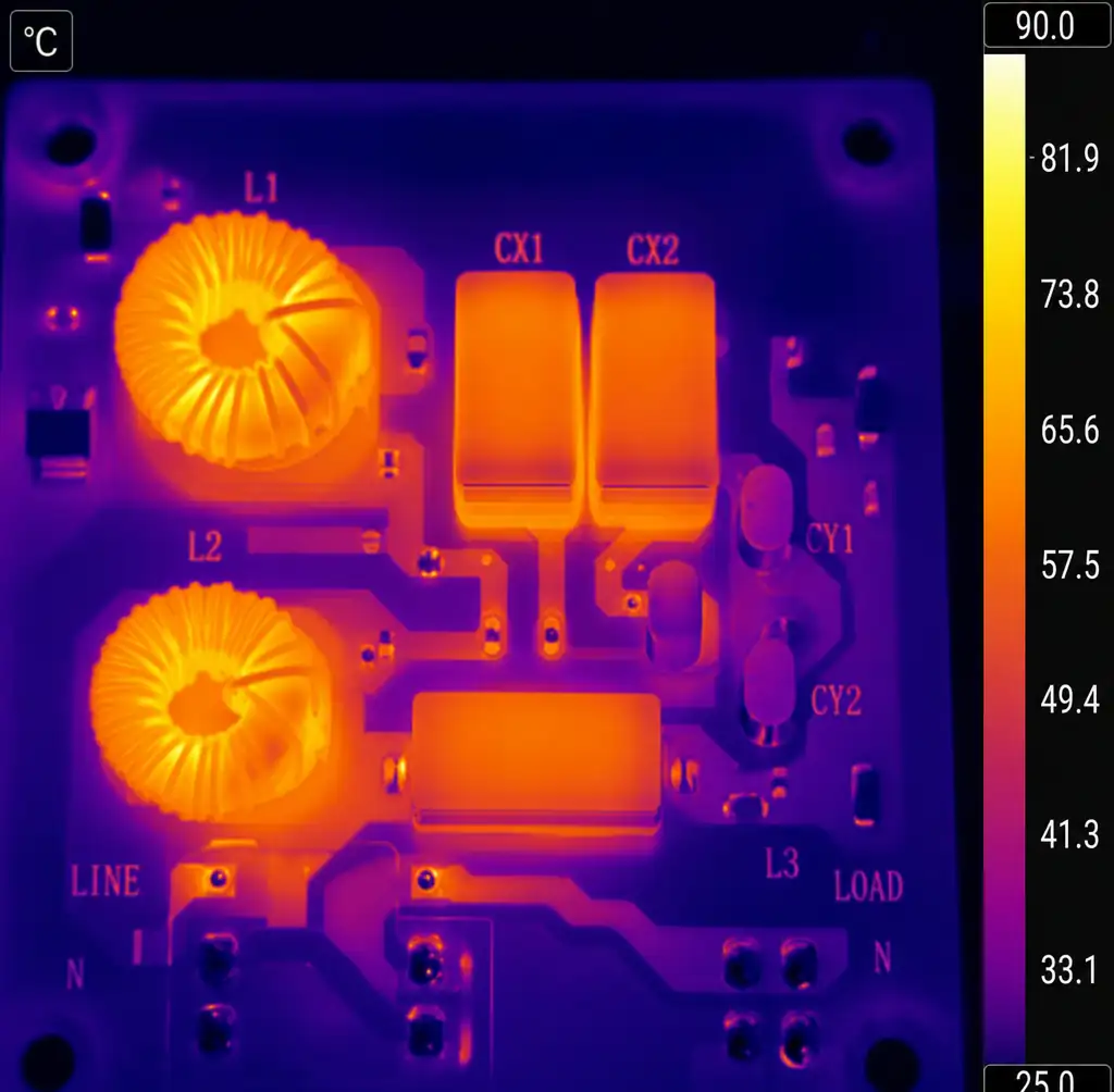 Thermal camera image showing heat distribution in EMI filter components under load
CM chokes carrying DC bias experience core heating from both copper loss and core loss. Core loss increases exponentially with flux density—operating at 80% of saturation flux generates 3-5x more heating than 50% operation. For reliability, derate inductor current to 70% of saturation rating and verify temperature rise under worst-case load conditions.
Voltage Derating Requirements
Safety standards mandate voltage derating for X and Y capacitors. Apply 60-70% derating factor to rated voltage—a 275 VAC X2 capacitor operates safely up to 165-190 VAC continuous. Transient voltage suppressors (TVs) or varistors protect against surge voltages during switching transients and lightning-induced events.
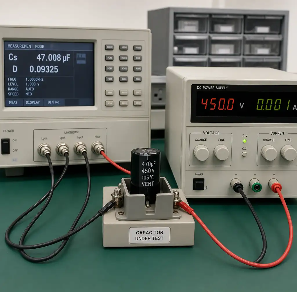 Test bench setup showing capacitor voltage coefficient measurement equipment
Ceramic capacitor voltage coefficient causes severe derating in high-K dielectrics. X7R 10 μF/25V capacitors retain only 4 μF at 25V DC bias. For DC link filtering in power supplies, use film capacitors for primary filtering and ceramics only for high-frequency bypassing where voltage coefficient has minimal impact.
7. FAQ
What is the difference between X and Y capacitors?
X-capacitors connect line-to-line (or line-to-neutral) for differential-mode filtering and do not create chassis leakage current. Y-capacitors connect line-to-ground for common-mode suppression but generate leakage current limited by safety standards. X-caps typically range 0.1-2.2 μF, while Y-caps remain in the 1-10 nF range to control leakage below regulatory limits.
How do I select between Mn-Zn and Ni-Zn ferrite cores?
Mn-Zn ferrites offer higher permeability (2,000-15,000) for maximum impedance at lower frequencies (150 kHz-10 MHz), making them ideal for conducted emissions filtering. Ni-Zn ferrites provide lower permeability (100-800) but maintain effectiveness to 200 MHz, suitable for high-frequency radiated emissions control. For broadband suppression, use Mn-Zn for primary filter stage and Ni-Zn for secondary high-frequency attenuation.
Can I use standard inductors instead of CM chokes?
Standard inductors filter differential-mode noise only and provide no common-mode suppression. Since common-mode currents dominate conducted emissions (typically 20-30 dB higher than DM), omitting CM chokes results in compliance failures. Cost savings from eliminating CM chokes are lost in redesign expenses and schedule delays.
Why does my filter perform worse on the PCB than in simulation?
Layout parasitics create unmodeled inductance and coupling. Input-to-output capacitive coupling through traces or ground plane discontinuities bypasses the filter. Long connection traces add series inductance reducing capacitor effectiveness. Shared ground return paths couple switching noise into filtered outputs. Successful EMI filtering requires equal attention to component selection and layout implementation.
What causes filter resonance and how do I dampen it?
Undamped LC filters create high-Q resonance amplifying emissions at resonant frequency by 10-30 dB. Add damping resistance in series with X-capacitors (typically 1-10 Ω) or use lossy ferrite beads with controlled impedance profiles. Resonance frequency must avoid critical compliance frequencies—if a 150 kHz resonance coincides with CISPR 25 peak limits, compliance becomes impossible without damping.
8. Conclusion
EMI/EMC compliance through component selection requires matching filter topology to noise characteristics, selecting capacitors and inductors based on high-frequency impedance behavior, and implementing PCB layouts that preserve component performance. Common-mode chokes with appropriate ferrite materials suppress the dominant emission mode, while proper X and Y capacitor selection balances filtering effectiveness against safety requirements.
For power electronics applications, prioritize Pi-section filters with damping networks and verify component specifications under actual voltage and temperature conditions. Layout execution determines whether theoretically sound designs achieve 40 dB attenuation or fail compliance by 6-10 dB margins.
Need help sourcing EMI/EMC certified components with test data and compliance documentation? Request a quote to discuss how our authorized manufacturer relationships support your EMC design requirements.