


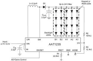
High Efficiency & Advanced Materials (Class D, GaN)
Introduction — Why efficiency and materials matter
Ever notice how your phone charger gets smaller every year while delivering more power? That’s not magic — that’s materials science and smarter topologies teaming up. When you combine Class D switching topologies with advanced materials like gallium nitride (GaN), you get dramatic efficiency, lower heat, and much higher power density. Want a compact amplifier, lightweight power supply, or high-frequency RF stage? This pairing is a fast lane.
Quick primer: What is a Class D amplifier?
Basic switching topology
Class D amplifiers aren’t “analog” in the usual sense. They switch transistors fully on or off, creating a pulse waveform that, after filtering, reconstructs the desired analog signal. Think of it like a high-speed light switch that modulates brightness so fast your eye sees a smooth dim level.
How PWM and modulation work
Pulse-width modulation (PWM) or other switching schemes encode amplitude in duty cycles or pulse patterns. The filtered output averages the pulses back into audio or power. Because the transistors spend most time fully on (low loss) or fully off (no conduction loss), conduction losses drop dramatically.
Key performance metrics for Class D
Efficiency (often >90% for well-designed systems) Total harmonic distortion + noise (THD+N) for audio Switching frequency and filter design Thermal performance and EMI Quick primer: What is GaN (gallium nitride)? Fundamental material properties GaN is a wide-bandgap semiconductor. Compared to silicon, GaN has higher electron mobility, higher breakdown field, and lower on-resistance at a given die size. In plain terms: it switches faster, handles higher voltages better, and wastes less energy as heat.
How GaN differs from silicon and SiC
vs. Silicon: faster switching, lower gate charge, lower conduction loss at high speed vs. SiC: SiC excels at very high voltages; GaN shines in high-frequency, medium-to-high voltage designs where speed and low capacitance matter
Why pair Class D with GaN?
Efficiency gains explained
Class D reduces switching loss by using on/off states, and GaN reduces those losses further because its switching transitions are cleaner and quicker. Fewer transition losses mean higher overall efficiency, sometimes by several percentage points — and that adds up in power-sensitive systems.
Power density and switching speed benefits
GaN tolerates higher frequency switching with less loss, letting designers push switching frequencies up. Higher frequency means smaller inductors and capacitors — which means smaller, lighter products. Imagine shaving inches off a power amplifier chassis or reducing the weight of an EV inverter module: that’s power density in action.
Design considerations when using GaN in Class D
Gate drive requirements and strategies
Unlike traditional MOSFETs, GaN FETs often need specialized gate drivers. Their lower gate charge and faster edges can cause instability or shoot-through if the driver isn’t matched properly. Use drivers designed for GaN, control slew rates, and consider dead-time strategies carefully.
Managing parasitic inductance and ringing
Fast transitions make stray inductance and capacitance more painful: ringing, overshoot, and EMI all grow. Keep loop areas tiny, use Kelvin connections, and add snubbers or RC dampers where appropriate. Think of the switching node as a rock concert — if everyone yells at once (fast edges) the sound (ringing) echoes unless you manage the stage.
EMI and filtering approaches
Higher switching speed shifts noise to higher frequencies, which are sometimes easier to filter but can also couple differently. Shielding, common-mode chokes, and careful filter placement are your friends. Also remember that smaller inductors are more sensitive to parasitic behavior.
Thermal management and heat sinking
Lower losses mean less heat, but hotspots still appear where switching occurs. Use thermal vias, direct copper pours, and consider metal-core PCBs or integrated heat spreaders for high-power modules. Thermal simulation early in the design can avoid late surprises.
PCB layout best practices
Minimize high di/dt loop areas Place gate driver close to FETs Separate power and signal grounds with a single star point Use wide traces and multiple vias for current paths Practical performance trade-offs Cost vs. benefit analysis GaN parts can be pricier per device than silicon, but system-level savings (smaller magnetics, smaller heatsinks, better efficiency) often offset the component cost. For volume products, GaN total cost of ownership frequently beats legacy solutions.
Reliability and ruggedness concerns
GaN technology has matured quickly, but its failure modes differ from silicon. Hard-switching abuse, voltage spikes, or improper gate drive can injure GaN more readily. Choose qualified parts, use protective networks, and design conservatively for surge events.
Failure modes and mitigation
Use TVS diodes or clamp networks to limit voltage overshoot Protect against gate overvoltage Add current limiting and diagnostics to detect early signs of stress
Applications that benefit most
High-performance audio amplifiers
Want a compact, cool-running amp with high efficiency? Class D with GaN can deliver audiophile-grade performance while slashing enclosure size and weight. Higher switching frequencies help push switching noise out of the audible band.
RF transmitters and base stations
For RF, switching speed and linearity are gold. GaN’s high electron mobility supports high-power RF stages with better efficiency and thermal robustness than silicon LDMOS in some scenarios.
Power supplies, class-D motor drives, EV inverters
From server PSUs to EV inverters, anywhere power density and efficiency matter, GaN-enabled Class D topologies can win. Higher frequency operation reduces passive component size, easing thermal and mechanical design.
Real-world examples and case studies
Power density wins: portable amplifiers
Companies shrinking portable speaker systems use GaN Class D to pack more punch into smaller enclosures. The result? Longer battery life and less heating during loud playback.
Efficiency wins: server power supplies
Data centers love efficiency. GaN-equipped DC-DC converters reduce losses and heat, translating directly into lower cooling costs and higher rack density.
Testing and measurement tips
Capturing fast switching waveforms
Use a low-inductance scope probe or a differential probe and keep probe ground leads extremely short. Otherwise, you’ll measure probe artifacts instead of true switching behavior.
Measuring efficiency correctly
Measure input power at the source and output power at the load, accounting for all auxiliary supplies. For Class D audio, test across different loads and frequencies; for power supplies, test across the load range and temperature extremes.
Future trends in materials and topology
Integration and monolithic solutions
Expect more GaN integration: gate drivers, synchronous control, and protection circuits co-packaged with the FETs. That reduces parasitics and simplifies layout — a tidy way to reclaim board real estate.
New wide-bandgap materials on the horizon
Beyond GaN and SiC, researchers are exploring materials and heterostructures that may push limits further. The goal: even faster switching, lower loss, and higher thermal tolerance.
Practical tips for engineers starting with GaN Class D
Start with reference designs from reputable vendors — they save weeks of trial and error. Use simulation (SPICE, electromagnetic) early, especially for EMI and thermal modeling. Invest in proper measurement tools: differential oscilloscope probes, current probes, and a good thermal camera. Prototype conservatively: add clamp networks and soft-start to protect devices during debugging.
Conclusion
Pairing Class D topologies with GaN devices is like replacing a bulky diesel engine with a turbocharged electric motor: same or better performance in a smaller, cooler, more efficient package. The marriage brings real-world benefits — higher efficiency, reduced size, and improved power density — but it asks designers to pay attention to gate driving, layout, and protection details. For engineers willing to learn the quirks, GaN-enabled Class D designs open doors to sleeker products and systems that run cooler and cleaner.
FAQs
Q1: How much efficiency improvement can I realistically expect by switching from silicon MOSFETs to GaN in a Class D design? A1: It depends on frequency, topology, and operating point, but typical system-level gains range from a few percentage points to 5–10% in switching loss-dominated designs. The real impact shows up in reduced cooling needs and smaller passives.
Q2: Are GaN devices harder to drive than silicon MOSFETs? A2: They’re different. GaN often needs specialized drivers or tighter gate control because of faster edges and lower gate charge. The goal is to control transition speed enough to prevent overshoot while preserving low loss.
Q3: Will GaN reduce EMI problems or make them worse? A3: It can go either way. Faster edges shift noise to higher frequencies, which may be easier to filter, but they also increase potential for ringing and common-mode noise. Good layout and filtering are essential.
Q4: Are there off-the-shelf integrated GaN Class D modules I can use to speed development? A4: Yes — several vendors offer reference modules and development kits with integrated drivers and protection. These are excellent starting points for proof-of-concept and layout learning.
Q5: Is GaN suitable for all voltage ranges? A5: GaN currently excels in low-to-medium high-voltage ranges (tens to a few hundred volts). For very high-voltage systems, SiC or other solutions may still be preferable. Always match device selection to system requirements.