


Infineon Automotive Gate Driver ICs | SiC/IGBT Motor Control Guide
Infineon automotive gate driver ICs serve as the critical bridge between low-voltage microcontroller signals and high-voltage power semiconductors in modern electric vehicle motor control systems. As the automotive industry accelerates toward electrification, these specialized integrated circuits have become indispensable for achieving the efficiency, safety, and reliability standards demanded by next-generation EV powertrains. Whether driving silicon IGBTs or next-generation SiC MOSFETs, Infineon's EiceDRIVER and MOTIX families deliver the precise gate control necessary to minimize switching losses while ensuring robust protection against fault conditions.
Quick Answer: Infineon automotive gate driver ICs are AEC-Q100 qualified integrated circuits that translate low-power PWM signals from microcontrollers into high-current gate drive outputs for power MOSFETs and IGBTs. They feature galvanic isolation, configurable dead-time control, integrated protection mechanisms (DESAT, OCP, UVLO), and SPI-based configurability, enabling optimized switching performance for SiC and IGBT power stages in traction inverters, DC-DC converters, and auxiliary motor drives up to 1200V.
Table of Contents
- 1. The Critical Challenge: Why Gate Driver Selection Defines Motor Control Performance
- 2. Infineon Gate Driver Portfolio: Matching the Right IC to Your Architecture
- 3. High-Side and Low-Side Driving: Fundamentals for Automotive Motor Control
- 4. SiC vs. IGBT Driving Strategies: Optimizing Switching Performance
- 5. Motor Control Efficiency Optimization: Practical Techniques
- 6. Step-by-Step Implementation Guide for Infineon Gate Drivers
- 7. Real-World Automotive Applications and Case Studies
- 8. Frequently Asked Questions About Infineon Gate Driver ICs
- 9. Conclusion: Driving the Future of Automotive Electrification
1. The Critical Challenge: Why Gate Driver Selection Defines Motor Control Performance
The electrification of automotive powertrains has placed unprecedented demands on power electronics design. Research data indicates that the global motor controllers market reached $37.99 billion in 2026, with projections showing expansion to $181.29 billion by 2035 at a CAGR of 18.8%. Within this rapidly growing landscape, gate driver IC selection has emerged as a decisive factor that directly impacts system efficiency, thermal management, and functional safety compliance.
1.1 The Efficiency Bottleneck in Power Stage Design
Power conversion losses in automotive traction inverters typically originate from three primary sources: conduction losses in the power semiconductor, switching losses during turn-on and turn-off transitions, and dead-time losses when both high-side and low-side switches are intentionally kept off. Analysis reveals that switching losses can account for 35-50% of total power dissipation in hard-switched inverter topologies operating at frequencies above 10 kHz. The gate driver's role in minimizing these losses is often underestimated by design engineers.
"Gate driver ICs are not simple buffer amplifiers. They are precision timing instruments that must deliver the exact charge profile to the power device's gate while maintaining nanosecond-level synchronization across isolation barriers." — Infineon Application Engineering Bulletin
The transition from silicon IGBTs to silicon carbide (SiC) MOSFETs has introduced additional complexity. SiC devices switch at dV/dt rates exceeding 50 V/ns, compared to 5-10 V/ns for conventional IGBTs. This dramatic increase in switching speed demands gate drivers with exceptional common-mode transient immunity (CMTI) and precisely controlled output stages to prevent shoot-through events and EMI degradation.
1.2 Functional Safety and Automotive Compliance Requirements
Modern automotive motor control systems must comply with ISO 26262 functional safety standards, often requiring ASIL D classification for safety-critical applications such as steer-by-wire and brake-by-wire systems. The gate driver IC assumes a pivotal role in this safety architecture by providing:
- Desaturation detection (DESAT) with configurable threshold levels and soft shutdown sequences
- Overcurrent protection (OCP) with programmable blanking times to prevent nuisance tripping
- Active short-circuit (ASC) capability for safe state entry during fault conditions
- Primary and secondary undervoltage lockout (UVLO) with hysteresis to ensure reliable startup
- SPI-based diagnostics providing real-time fault reporting to the system microcontroller
| Parameter | ASIL B Requirements | ASIL D Requirements |
|---|---|---|
| Single-point fault metric | > 90% | > 99% |
| Latent fault metric | > 60% | > 90% |
| Diagnostic coverage | Medium (80-90%) | High (90-99%) |
| Gate driver response time | < 10 µs | < 5 µs |
| Required safety documentation | FMEDA | Full safety manual + FMEDA |
Note: Infineon's EiceDRIVER 1EDI305xAS family provides comprehensive safety documentation through the myICP platform, including pre-calculated FMEDA templates that can reduce safety analysis effort by up to 60% compared to discrete gate drive solutions.
1.3 Market Dynamics Driving Gate Driver Innovation
The automotive isolated gate driver IC market was valued at $106 million in 2025, with forecasts projecting growth to $167 million by 2034 at a 6.9% CAGR. This growth trajectory correlates directly with SiC adoption rates in traction inverters, which are experiencing approximately 25% CAGR through 2030.
"The projected 25% CAGR for SiC devices in automotive applications through 2030 creates significant demand for next-generation isolated gate driver ICs optimized for 800V architectures." — Automotive Isolated Gate Driver IC Market Outlook 2026-2034, Industry Research Report
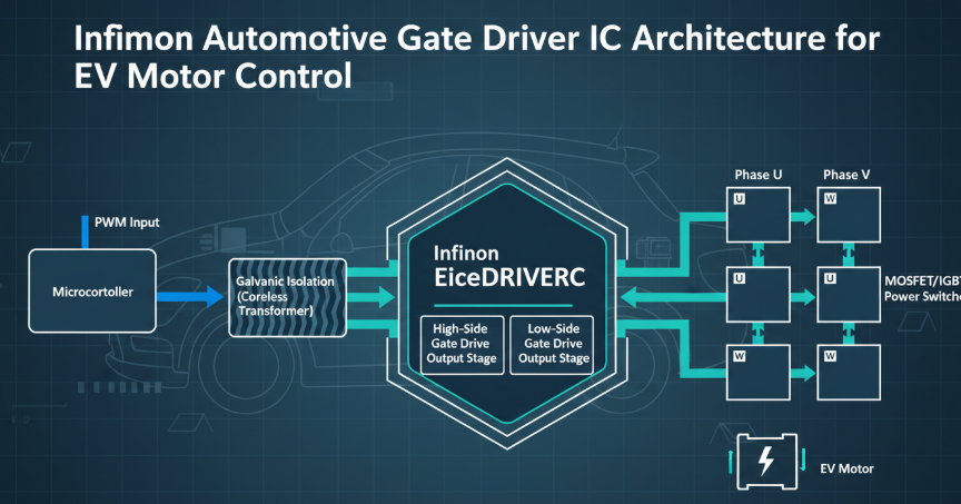
Figure 1: Infineon EiceDRIVER Architecture with Coreless Transformer Isolation for EV Motor Control Applications
2. Infineon Gate Driver Portfolio: Matching the Right IC to Your Architecture
Infineon offers a comprehensive portfolio of automotive-qualified gate driver ICs organized into two primary families: EiceDRIVER for high-voltage isolated applications (xEV traction inverters, onboard chargers, DC-DC converters) and MOTIX for low-voltage motor control (12V/48V auxiliary motors, pumps, fans, EPS systems).
2.1 EiceDRIVER Family: High-Voltage Isolated Gate Drivers for xEV Applications
The EiceDRIVER isolated gate driver ICs utilize Infineon's proprietary coreless transformer (CT) technology to achieve galvanic isolation with bidirectional signal transmission. This technology eliminates the need for optocouplers or bulky magnetic transformers, resulting in compact packages with exceptional noise immunity.
| Product Family | Voltage Class | Output Current | Isolation | Key Features |
|---|---|---|---|---|
| 1EDI302xAS | 1200V | 12A source/sink | Reinforced (CT) | SPI interface, DESAT, 60ns propagation delay |
| 1EDI303xAS | 1200V | 12A source/sink | Reinforced (CT) | SiC-optimized, extended CMTI, wide output supply range |
| 1EDI305xAS | 1200V | 20A source/sink | Reinforced (CT) | SiC-optimized, dual Miller clamp, integrated flyback controller, dual ADC |
The 1EDI3050AS represents the flagship device for high-power automotive motor drives above 50 kW. Key specifications include:
- 20A peak output current with rail-to-rail split output stage
- Dual integrated Miller clamp with 5A capability plus external clamp transistor support
- CMTI up to 150 V/ns at 1000V operating conditions
- 8kV basic insulation per DIN EN IEC 60747-17 (VDE 0884-17)
- Integrated flyback controller for optimized supply architecture
- Dual 12-bit ADC for temperature and DC-link voltage measurement
- Operating temperature range: -40°C to +150°C ambient
2.2 MOTIX Family: Low-Voltage Motor Gate Drivers for Auxiliary Applications
The MOTIX portfolio addresses the diverse requirements of 12V and 48V automotive motor control applications, from brushed DC motors in body electronics to brushless DC motors in safety-critical steering and braking systems.
| Product | Supply Voltage | Channels | Safety Rating | Target Applications |
|---|---|---|---|---|
| TLE9189QVW | 4.2V - 36V | 3-phase | ASIL D (ISO 26262) | EPS, brake-by-wire, steer-by-wire |
| TLE9186QVW | 4.2V - 36V | 3-phase | ASIL B | Thermal management, body applications |
| TLE92104/8 | 12V | 8 half-bridges | ISO 26262-ready | Seat control, window lift, power liftgate |
| TLE956x | 12V | Integrated SBC | ASIL B | BDC/BLDC motor system IC with CAN/LIN |
Key Insight: The MOTIX TLE9189QVW features Infineon's patented adaptive MOSFET control technology, which automatically measures and compensates for MOSFET switching characteristics. This eliminates end-of-line calibration requirements and optimizes the balance between power dissipation and EMC performance across production variations.
2.3 Selection Decision Matrix
Selecting the right Infineon automotive gate driver ICs for your design depends on several critical system-level parameters:
- Bus voltage: Applications above 60V require EiceDRIVER isolated drivers; below 60V can use MOTIX level-shifter drivers
- Power level: Traction inverters above 50kW demand the 20A output capability of 1EDI305xAS devices
- Safety classification: ASIL D systems require drivers with comprehensive diagnostic coverage (TLE9189QVW or 1EDI305xAS)
- Power switch technology: SiC MOSFETs require drivers with extended CMTI (>100 V/ns) and negative gate voltage capability
- Communication interface: Systems requiring runtime configurability benefit from SPI-capable devices
3. High-Side and Low-Side Driving: Fundamentals for Automotive Motor Control
Understanding high-side and low-side driving fundamentals is essential when designing systems with Infineon automotive gate driver ICs for robust motor control performance. The gate driver must not only deliver sufficient charge to switch the power device within the required time but also maintain proper voltage levels relative to the switching node potential.
3.1 Bootstrap Supply Design for High-Side Drivers
In half-bridge and three-phase inverter configurations, the high-side gate driver must generate gate drive voltages referenced to the switching node (VS) rather than ground. This is typically accomplished using a bootstrap supply circuit consisting of a diode and capacitor connected to a low-voltage supply.
Key design considerations for bootstrap operation include:
- Bootstrap capacitor sizing: The capacitor must supply sufficient charge for the high-side gate drive without excessive voltage droop during the switching cycle. Calculate using: C_boot > (2 × Q_g + I_q × t_on + Q_ls) / ΔV_boot, where Q_g is the total gate charge, I_q is the high-side quiescent current, and Q_ls represents level-shift charge requirements
- Bootstrap diode selection: Use fast-recovery or Schottky diodes with reverse voltage rating exceeding the DC-link voltage
- Refresh time constraints: The bootstrap capacitor must be recharged during the low-side conduction period; minimum duty cycle limitations apply
- Startup sequencing: Initial bootstrap capacitor charging requires a specific PWM pattern before normal operation commences
3.2 Dead-Time Management and Shoot-Through Prevention
Shoot-through occurs when both high-side and low-side switches conduct simultaneously, creating a low-impedance path across the DC-link capacitor. This condition can destroy power devices within microseconds. Infineon gate drivers address this risk through multiple mechanisms:
- Integrated dead-time insertion: Programmable dead-time from 100ns to several microseconds prevents simultaneous conduction
- Cross-conduction prevention logic: Hardware interlocks ensure that a turn-on command for one switch forces the complementary switch to turn off first
- Separate source/sink outputs: Split output stages allow independent optimization of turn-on and turn-off gate resistances
- Adaptive dead-time control: Advanced drivers monitor the actual switch timing and automatically adjust dead-time to minimize conduction losses while maintaining safety margins
Practical Tip: When designing with SiC MOSFETs, recommended dead-time settings are typically shorter than for IGBTs due to the absence of tail current. Infineon's 1EDI303xAS family supports internal dead-times as low as 50ns, enabling higher effective duty cycles and improved DC-link voltage utilization.
3.3 Ground Bounce and Noise Immunity
High dI/dt during switching transitions induces voltage transients across parasitic inductances in the gate drive loop. This phenomenon, known as ground bounce, can cause spurious turn-on or insufficient turn-off voltage if not properly managed.
Infineon's automotive gate drivers incorporate several features to enhance noise immunity:
- Separate power and signal ground pins: Physical isolation between high-current output returns and sensitive logic grounds
- Hysteretic input thresholds: Input logic with 0.4V minimum hysteresis prevents false triggering from noise coupling
- Integrated negative voltage clamping: Protection against undershoot transients down to -5V on gate drive outputs
- High CMTI specification: >300 kV/µs immunity on 1ED301xMC12I family ensures reliable operation in fast-switching SiC environments
4. SiC vs. IGBT Driving Strategies: Optimizing Switching Performance
The choice between SiC MOSFET and IGBT power switches fundamentally changes the requirements for Infineon automotive gate driver ICs. While both devices are voltage-controlled, their switching characteristics, gate charge profiles, and protection needs differ significantly.
4.1 Comparative Analysis: Key Driving Differences
| Parameter | Si IGBT Driving | SiC MOSFET Driving | Design Implication |
|---|---|---|---|
| Gate voltage (turn-on) | +15V typical | +18V recommended | Higher output supply range required |
| Gate voltage (turn-off) | 0V to -5V | -2V to -5V preferred | Negative gate bias supply needed |
| Switching speed | 50-200 ns transitions | 10-50 ns transitions | Requires higher CMTI (>100 V/ns) |
| Gate charge (Q_g) | Higher | Lower | Less drive power but faster dV/dt |
| Miller plateau | Pronounced | Shorter | Reduced Miller effect but more sensitive to noise |
| Short-circuit withstand | 5-10 µs | 1-3 µs | Faster protection response required |
| Tail current | Present | Absent | Lower switching losses, no tail-related dead-time constraints |
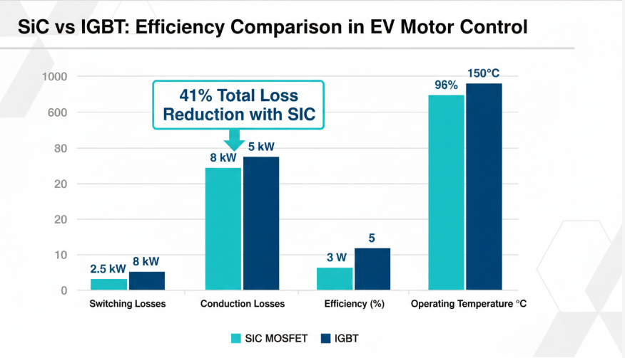
Figure 2: SiC MOSFET vs. IGBT Efficiency Comparison Data for EV Traction Inverter Applications
4.2 SiC-Optimized Gate Driver Features
Infineon's 1EDI303xAS and 1EDI305xAS families incorporate specific optimizations for SiC MOSFET driving:
- Extended CMTI capability: Tested to 150 V/ns for reliable operation at maximum SiC switching speeds
- Wide output-side supply range: Supports bipolar supply configurations up to +20V/-5V for optimal SiC gate drive
- Short internal dead-time: 50ns minimum dead-time enables higher modulation index and better DC-link utilization
- DESAT/OCP threshold adaptation: Programmable desaturation detection levels accommodate SiC MOSFET's different saturation characteristics
- Active Miller clamp: Dual integrated Miller clamp with 5A capability prevents false turn-on during high dV/dt transitions
- Separate source/sink outputs: Independent control of turn-on and turn-off gate resistances for precise switching waveform shaping
Performance Data: Testing with the WLPT driving cycle profile demonstrates that SiC power stages with optimized gate driving can achieve efficiency gains of up to 2% compared to IGBT-based designs. This translates to approximately 7 additional miles of driving range per battery charge, accumulating to over 1,000 extra miles annually for typical EV users.
4.3 IGBT Driving Considerations
Despite the momentum behind SiC adoption, IGBTs remain cost-effective solutions for applications where switching frequencies remain below 20 kHz and efficiency requirements are less stringent. Infineon's 1EDI302xAS family is specifically optimized for IGBT driving:
- Two-level turn-off (TLTO) capability for soft shutdown during fault conditions
- Programmable active clamping for collector voltage limitation
- DESAT detection with fully configurable blanking time and shutdown slope
- Support for active short-circuit (ASC) implementation strategies
Design Trade-off: While SiC MOSFETs offer superior efficiency and thermal performance, they typically carry a 2-3x premium in device cost compared to equivalent-rated IGBTs. For 400V architectures with moderate power requirements (< 100 kW), IGBT solutions with optimized gate driving can provide compelling system cost efficiency while meeting performance targets.
5. Motor Control Efficiency Optimization: Practical Techniques
Optimizing motor control efficiency with Infineon automotive gate driver ICs requires a holistic approach encompassing gate drive strength, switching timing, thermal management, and control algorithm tuning. Infineon's gate driver ICs provide the configurability necessary to implement these optimizations at the hardware level.
5.1 Dynamic Gate Drive Strength Control
The ability to adjust gate drive current in real-time enables significant efficiency improvements across varying operating conditions. The principle is straightforward:
- High gate drive strength during heavy load conditions minimizes switching losses by reducing transition times
- Reduced gate drive strength during light load conditions mitigates voltage overshoot and ringing, improving EMI while maintaining acceptable switching losses
Infineon's EiceDRIVER 1EDI305xAS family implements this through SPI-configurable output stage current, allowing dynamic adjustment without hardware modifications. Test data demonstrates that variable gate drive strength can:
- Reduce switching losses by 15-25% at high load points compared to fixed moderate drive
- Decrease voltage overshoot by 30-40% during light load operation
- Extend maximum switching frequency capability by optimizing rise/fall time trade-offs
5.2 Switching Frequency Optimization
Selecting the optimal switching frequency involves balancing multiple competing factors:
| Factor | Low Frequency (< 10 kHz) | High Frequency (> 20 kHz) |
|---|---|---|
| Switching losses | Lower | Higher |
| Current ripple | Higher | Lower |
| Motor iron losses | Higher | Lower |
| Audible noise | Present | Eliminated |
| Filter/component size | Larger | Smaller |
| Control bandwidth | Lower | Higher |
SiC MOSFETs enable operation at frequencies above 40 kHz without prohibitive switching losses, whereas IGBT designs are typically constrained to 10-15 kHz for traction inverter applications. The faster switching capability of SiC, combined with optimized gate driving, allows designers to push switching frequencies into the ultrasonic range, eliminating audible whine while maintaining or improving system efficiency.
5.3 Thermal Management and Power Stage Layout
Gate driver selection directly impacts thermal management requirements through its influence on switching losses. Consider the following thermal analysis for a 150 kW traction inverter:
- IGBT solution with standard gate driving: ~2.5 kW total switching losses, requiring liquid cooling with 8 L/min flow rate
- SiC solution with optimized gate driving: ~1.2 kW total switching losses, enabling either reduced coolant flow (4 L/min) or smaller heat exchanger
This 52% reduction in switching losses translates directly to improved system power density and reduced thermal management cost and complexity.
Thermal Design Tip: Place the gate driver IC as close as possible to the power device gate terminals to minimize parasitic inductance in the gate drive loop. Infineon's compact DSO-20 and DSO-36 packages enable placement within 10mm of the power module, reducing gate loop inductance to < 5 nH for optimal switching performance.
5.4 Dead-Time Compensation in Control Algorithms
Fixed dead-time insertion creates voltage distortion and current zero-crossing distortion, particularly problematic at low modulation indices. Advanced motor control systems implement adaptive dead-time compensation:
- Current-direction-based compensation: The control algorithm estimates the current polarity and adjusts the commanded duty cycle to counteract dead-time voltage error
- Online parameter estimation: The system continuously estimates the actual dead-time and device voltage drop, updating compensation tables in real-time
- Feedforward compensation: Using pre-calibrated dead-time voltage characteristics based on operating conditions
Infineon gate drivers with SPI configurability enable runtime dead-time adjustment, allowing the control algorithm to minimize dead-time during low-current operation (where shoot-through risk is reduced) while maintaining conservative margins during high-current transients.
6. Step-by-Step Implementation Guide for Infineon Gate Drivers
Successful integration of Infineon automotive gate driver ICs into production designs requires a systematic approach spanning electrical design, PCB layout, software configuration, and validation testing.
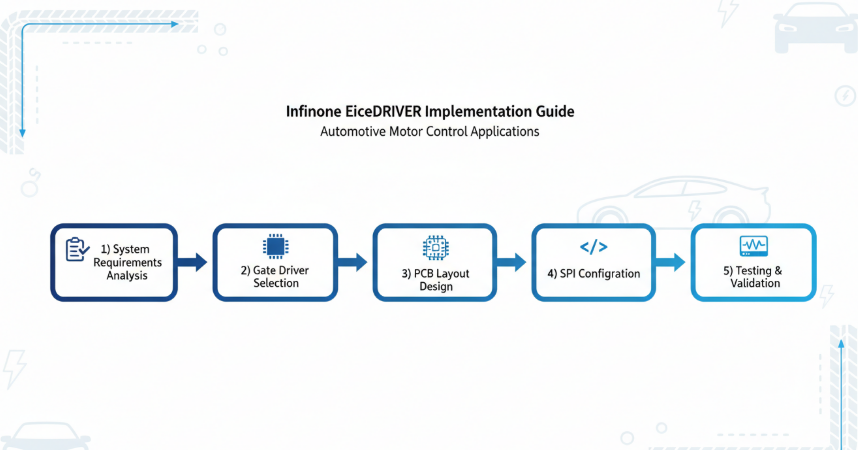
Figure 3: Infineon EiceDRIVER Implementation Workflow for Automotive Motor Control Design
Step 1: Define System Requirements and Constraints
Begin by documenting all system-level parameters that influence gate driver selection:
- Power stage topology: Half-bridge, three-phase inverter, or multi-level configuration
- DC-link voltage range: Including transient conditions during regenerative braking
- Power switch technology: SiC MOSFET, IGBT, or parallel combinations
- Peak and continuous output current requirements
- Switching frequency target: Based on efficiency, audible noise, and control bandwidth requirements
- Functional safety classification: ASIL A through ASIL D per ISO 26262
- Ambient temperature range: Including under-hood thermal conditions (-40°C to +150°C)
- EMC requirements: CISPR 25 Class 5 or equivalent emission and immunity standards
Step 2: Select the Appropriate Gate Driver IC
Using Infineon's online selection tool or parametric search:
- Filter by voltage class (600V, 1200V, or 1700V)
- Select isolation type (functional, basic, or reinforced per system safety requirements)
- Choose output current capability based on gate charge and switching time requirements
- Verify safety features match functional safety classification needs
- Confirm package compatibility with power module or discrete device layout
- Evaluate evaluation board availability and design support resources
Step 3: Design the Gate Drive Circuit and PCB Layout
Critical PCB layout guidelines for optimal gate drive performance:
- Minimize gate loop inductance: Keep gate driver output traces short and wide (< 10mm length, > 0.5mm width)
- Kelvin source connection: Connect gate driver ground directly to the power device source pin, not to the main power return path
- Bootstrap capacitor placement: Position within 2mm of the bootstrap and VS pins with minimal trace length
- Decoupling capacitors: Use parallel ceramic capacitors (100nF + 10µF) placed immediately adjacent to supply pins
- Isolation barrier maintenance: Ensure adequate creepage and clearance distances per IEC 60664-1 for the working voltage
- Thermal vias: Implement thermal via arrays under the exposed pad for DSO packages, connecting to internal ground planes
Step 4: Configure Gate Driver Parameters via SPI
Infineon's EiceDRIVER devices with SPI interface enable comprehensive runtime configurability
Step 5: Validation and Characterization Testing
Comprehensive test protocol for gate driver validation:
- Double-pulse testing: Characterize switching waveforms across current and temperature range
- Dead-time verification: Measure actual dead-time with oscilloscope and adjust as needed
- Protection feature testing: Verify DESAT, OCP, and UVLO response under fault injection
- Thermal characterization: Monitor driver junction temperature at maximum operating conditions
- EMC pre-compliance: Conduct conducted and radiated emission scanning per CISPR 25
- Functional safety validation: Execute fault injection campaign per ISO 26262-5 requirements
7. Real-World Automotive Applications and Case Studies
Infineon automotive gate driver ICs are deployed across the full spectrum of electrified vehicle powertrain applications, from mild-hybrid systems to full battery electric vehicles.
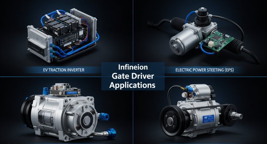
Figure 4: Infineon Gate Driver IC Applications Across Automotive Electrification Systems
Case Study 1: 800V Traction Inverter with SiC Power Module
A Tier 1 automotive supplier implemented a 200 kW traction inverter for a premium EV platform using Infineon's 1EDI3050AS gate drivers paired with CoolSiC MOSFET power modules.
System specifications:
- DC-link voltage: 800V (nominal), 850V (maximum)
- Peak output current: 450A RMS
- Switching frequency: 16 kHz (IGBT baseline) → 24 kHz (SiC optimized)
- Cooling: Liquid-cooled cold plate with 65°C coolant inlet
Results achieved:
- System efficiency improvement: 97.2% peak efficiency (vs. 95.1% with previous IGBT design)
- Power density increase: 35 kW/L (vs. 22 kW/L with IGBT)
- Switching loss reduction: 68% at rated operating point
- Thermal management simplification: Reduced coolant flow requirement by 40%
- Functional safety: Achieved ASIL D with integrated safety features
"The 1EDI3050AS integrated flyback controller simplified our auxiliary supply architecture significantly. We eliminated three external power supply ICs and reduced PCB area by 25% compared to our previous discrete gate drive design." — Power Electronics Design Lead, Tier 1 Automotive Supplier
Case Study 2: Electric Power Steering (EPS) System
An EPS module manufacturer selected the MOTIX TLE9189QVW for a safety-critical steer-by-wire application requiring ASIL D compliance.
Key design challenges addressed:
- Diagnostic coverage requirements: TLE9189QVW's integrated monitoring functions for gate driver, inverter, microcontroller, and MCU interfaces provided comprehensive fault coverage
- EMC optimization: Adaptive MOSFET control automatically tuned switching characteristics across production spread, eliminating end-of-line calibration
- Current sensing accuracy: Three integrated current sense amplifiers with programmable gain enabled precise torque control without external sense resistors
- Safety validation: Built-in self-test functions with low FIT rates accelerated ISO 26262 compliance certification
Measured performance:
- Gate drive rise/fall time consistency: ±3% across temperature and MOSFET variation
- EMC margin: > 6 dB below CISPR 25 Class 5 limits
- System availability: > 99.99% with comprehensive diagnostic coverage
Case Study 3: 48V Mild-Hybrid Belt-Driven Starter Generator (BSG)
A 48V mild-hybrid system utilized MOTIX TLE9140EQW gate drivers for the integrated starter-generator application, delivering 15 kW of boost/recuperation power.
System architecture highlights:
- 48V lithium-ion battery with 52V maximum charge voltage
- Air-cooled power stage with 150°C maximum junction temperature
- Sensorless field-oriented control (FOC) with 10 kHz switching frequency
- ASIL B functional safety requirement for torque safety
Efficiency optimization results:
- Peak system efficiency: 96.8% at 30 kW/m³ power density
- Adaptive gate control reduced switching losses by 12% compared to fixed drive strength
- Integrated protection features prevented three potential field failures during 500,000 km equivalent durability testing
Case Study 4: High-Voltage DC-DC Converter for EV Auxiliary Systems
An onboard DC-DC converter (400V/12V, 3kW) employed 1EDI3021AS gate drivers with IGBT power devices for cost-sensitive mass-market EV applications.
Design outcomes:
- Achieved 94.5% peak efficiency at 50% load point
- DESAT protection successfully triggered during output short-circuit test, protecting IGBTs from destruction
- Compact DSO-20 package enabled 45% reduction in gate drive PCB area compared to optocoupler-based solution
- Total BOM cost reduction of $2.80 per channel vs. legacy implementation
8. Frequently Asked Questions About Infineon Gate Driver ICs
What are the key differences between Infineon EiceDRIVER and MOTIX gate driver families?
EiceDRIVER is Infineon's family of isolated gate drivers designed for high-voltage applications (600V-1200V) in xEV powertrains. These devices feature coreless transformer isolation, support IGBT and SiC MOSFET technologies, and include comprehensive safety features for ASIL D systems. MOTIX comprises low-voltage gate drivers (< 100V) for 12V and 48V automotive auxiliary motors, integrating features like adaptive MOSFET control, current sense amplifiers, and system basis chip (SBC) functionality for body electronics and safety-critical applications.
How does Infineon's coreless transformer (CT) isolation technology compare to optocoupler-based solutions?
Infineon's CT technology offers several advantages over traditional optocouplers:
- Superior timing performance: Propagation delays as low as 40ns with < 10ns part-to-part matching (vs. 100-500ns for optocouplers)
- Higher CMTI: > 300 kV/µs immunity (vs. typically 15-50 kV/µs for optocouplers)
- Longer service life: No LED degradation over time; performance stable across temperature and aging
- Reduced PCB area: Compact DSO packages eliminate bulky optocoupler footprints and associated discrete components
- Enhanced reliability: Eliminates optocoupler's inherent CTR (current transfer ratio) variation and aging concerns
What SiC-specific features do Infineon gate drivers provide for traction inverter applications?
The 1EDI303xAS and 1EDI305xAS families include specific optimizations for SiC MOSFET driving:
- Extended CMTI capability to 150 V/ns for reliable high-speed switching
- Wide output supply range supporting +18V/-5V bipolar gate drive configurations
- Short internal dead-time (50ns minimum) for maximum duty cycle utilization
- Dual integrated Miller clamp with 5A capability to prevent false turn-on
- DESAT threshold adaptation for SiC MOSFET saturation characteristics
- 20A peak output current for driving large-area SiC devices with fast switching transitions
How can I evaluate Infineon gate drivers for my automotive motor control design?
Infineon provides comprehensive design-in support including:
- Evaluation boards: Available for all major gate driver families with pre-configured test setups
- Graphical user interface (GUI): PC-based tool for real-time SPI register configuration and monitoring
- Application notes: Detailed documentation covering layout guidelines, protection tuning, and safety implementation
- Simulation models: SPICE and Simplis models for circuit simulation and verification
- Safety documentation: FMEDA, safety manuals, and safety analysis reports accessible via myICP portal (registration required)
- Reference designs: Complete system solutions demonstrating optimal gate driver integration
What functional safety documentation does Infineon provide for ISO 26262 compliance?
Infineon offers extensive safety documentation through the myICP information exchange platform:
- Safety Manual with detailed safety mechanism descriptions
- Failure Modes, Effects, and Diagnostics Analysis (FMEDA) with quantitative failure rates
- Safety Analysis Report confirming safety mechanism effectiveness
- Application-level safety guides for ASIL D implementation
- Pin Failure Mode Analysis (PFM) for systematic fault consideration
These documents can reduce safety analysis effort by up to 60% compared to developing safety concepts from scratch with discrete components.
9. Conclusion: Driving the Future of Automotive Electrification
Infineon automotive gate driver ICs represent a cornerstone technology in the ongoing transformation of automotive power electronics. From the high-voltage EiceDRIVER family enabling SiC-based traction inverters to the MOTIX portfolio addressing the diverse needs of auxiliary motor control, these devices provide the precision, protection, and configurability required by modern electrified powertrains.
Analysis of market trends and technology roadmaps indicates three converging forces that will continue to drive gate driver innovation:
- SiC adoption acceleration: With SiC traction inverter deployments growing at 25% CAGR, demand for optimized gate drivers with extended CMTI and faster switching capability will intensify
- 800V architecture migration: Next-generation EV platforms adopting 800V battery systems require gate drivers with reinforced isolation and higher voltage ratings
- Functional safety escalation: The proliferation of by-wire systems (steer-by-wire, brake-by-wire) is pushing gate driver safety requirements from ASIL B to ASIL D across an expanding range of applications
For design engineers, the key takeaway is that gate driver selection is not a late-stage implementation detail but a fundamental architectural decision that cascades through efficiency, thermal management, safety compliance, and ultimately system cost. Infineon's portfolio of AEC-Q100 qualified devices, supported by comprehensive design resources and safety documentation, provides a proven foundation for addressing these challenges.
"The difference between a good motor control design and an exceptional one often comes down to gate drive optimization. The 2% efficiency improvement achievable with proper SiC gate driving translates to millions of dollars in battery cost savings at production volumes." — Automotive Power Electronics Engineering Analysis
The data is clear: optimized gate driving with Infineon's automotive-qualified ICs delivers measurable improvements in efficiency, power density, and safety compliance. As the industry moves toward 2025-2030 electrification targets, these incremental improvements in power stage performance will collectively determine which platforms achieve cost and performance leadership in the marketplace.