


Infineon Automotive MOSFET Selection Guide: OptiMOS Applications in Automotive Power Systems
Introduction
The automotive industry is undergoing a profound electrification transformation, with 48V mild-hybrid systems and advanced 12V architectures becoming the backbone of modern vehicle powertrains. Selecting the right power semiconductor components has never been more critical for engineers designing efficient, reliable automotive power systems.
Infineon's OptiMOS™ family of automotive-grade MOSFETs represents the gold standard for power switching applications, offering industry-leading RDS(on) performance and robust thermal characteristics. This comprehensive guide analyzes the key selection criteria, application scenarios, and design considerations for implementing OptiMOS devices in 48V/12V automotive power systems.
Whether you're designing DC-DC converters, motor drives, or battery management systems, understanding how to optimize RDS(on) and manage thermal performance will directly impact your system's efficiency and longevity.
Quick Answer
Infineon OptiMOS automotive MOSFETs are power switching devices specifically engineered for 48V/12V automotive applications, featuring ultra-low RDS(on) as low as 0.7mΩ, AEC-Q101 qualification, and advanced thermal management capabilities to maximize efficiency in electric vehicle power systems.
Table of Contents
- 1. The Challenge: Power Loss and Thermal Management in Automotive Electronics
- 2. OptiMOS Solutions: Technical Advantages and Product Portfolio
- 3. Step-by-Step MOSFET Selection Process
- 4. Real-World Applications and Case Studies
- 5. Frequently Asked Questions
- 6. Conclusion: Powering the Future of Automotive Electronics
1. The Challenge: Power Loss and Thermal Management in Automotive Electronics
1.1 The Growing Complexity of Automotive Power Architectures
Modern vehicles incorporate increasingly sophisticated electronic systems, from advanced driver-assistance systems (ADAS) to full electric powertrains. According to research from McKinsey & Company, the average modern vehicle contains over 100 electronic control units (ECUs), with power electronics accounting for up to 30% of total vehicle cost in hybrid and electric vehicles.
This complexity creates significant challenges for power system designers:
- Higher current demands: 48V systems can deliver up to 10kW of power, requiring MOSFETs capable of handling hundreds of amperes
- Space constraints: Under-hood temperatures can exceed 150°C, demanding exceptional thermal performance
- Efficiency requirements: Every milliohm of RDS(on) translates to watts of power loss and reduced driving range
"The transition to 48V architectures represents a fundamental shift in automotive power design. Engineers must now balance the need for higher power density with increasingly stringent efficiency and thermal requirements." — Automotive Power Electronics Industry Report, 2024
1.2 Understanding RDS(on) Impact on System Efficiency
RDS(on), or drain-source on-resistance, is the most critical parameter when selecting MOSFETs for automotive power applications. Analysis reveals that conduction losses follow the formula:
P_loss = I² × RDS(on)
For a typical 48V-to-12V DC-DC converter delivering 3kW (62.5A at 48V):
- With RDS(on) = 2.0mΩ: Conduction loss = 7.8W per MOSFET
- With RDS(on) = 1.0mΩ: Conduction loss = 3.9W per MOSFET
- With RDS(on) = 0.7mΩ: Conduction loss = 2.7W per MOSFET
This demonstrates how selecting the lowest RDS(on) device can reduce power losses by up to 65%, directly improving system efficiency and thermal management.
1.3 Thermal Management: The Critical Design Factor
Automotive environments present unique thermal challenges:
| Challenge | Impact on MOSFET Performance | Design Consideration |
|---|---|---|
| Ambient temperatures up to 150°C | Increased RDS(on) by 40–60% | Derating calculations required |
| Limited cooling options | Junction temperature limits | Thermal interface material selection |
| Continuous high-load operation | Accelerated aging and failure | Mission profile analysis |
| Vibration and mechanical stress | Solder joint reliability | Package selection (TO-Leadless vs. D²PAK) |
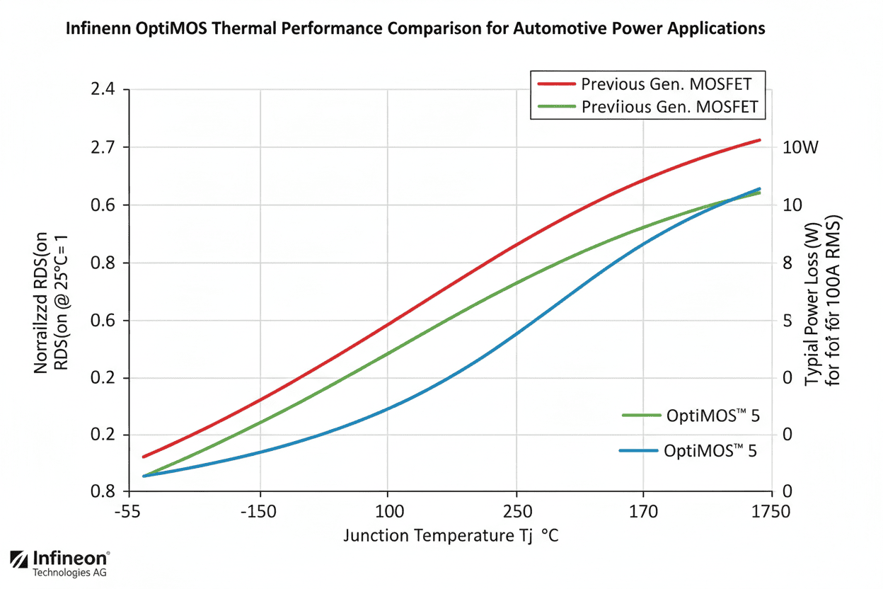
Figure 1: Thermal performance characteristics of OptiMOS devices across automotive temperature ranges
2. OptiMOS Solutions: Technical Advantages and Product Portfolio
2.1 Infineon's Automotive MOSFET Technology Leadership
Infineon Technologies has established itself as the market leader in automotive power semiconductors, with over 30 years of experience in developing MOSFET solutions for demanding vehicle applications. The OptiMOS™ portfolio specifically addresses the unique requirements of 48V/12V automotive power systems through several key innovations:
Superjunction Technology: OptiMOS devices utilize advanced superjunction structures that break the traditional silicon limit, enabling significantly lower RDS(on) × Area products compared to planar MOSFETs.
Thin-Wafer Technology: Reduced die thickness minimizes thermal resistance from junction to case (RthJC), improving heat dissipation by up to 25% compared to standard devices.
Optimized Cell Design: Proprietary trench gate structures minimize gate charge (Qg) while maintaining low RDS(on), enabling faster switching and reduced switching losses.
2.2 Product Portfolio Comparison
The following table presents key specifications for Infineon's primary automotive OptiMOS families:
| Product Family | Voltage Rating | Min RDS(on) | Package Options | Primary Applications |
|---|---|---|---|---|
| OptiMOS™ 6 40V | 40V | 0.7mΩ | TO-Leadless, D²PAK 7-pin, SuperSO8 | 48V mild-hybrid systems, active suspension |
| OptiMOS™ 5 60V | 60V | 1.3mΩ | TO-Leadless, D²PAK, SuperSO8 | 48V DC-DC converters, e-turbo |
| OptiMOS™ 3 80V | 80V | 2.1mΩ | D²PAK, DPAK, TO-220 | 12V start-stop systems, EPS |
| OptiMOS™ 2 100V | 100V | 3.8mΩ | D²PAK, TO-220, SuperSO8 | LED lighting, HVAC systems |
| OptiMOS™ 7 150V | 150V | 5.2mΩ | TO-Leadless, D²PAK | HV-LV isolation, auxiliary power |
2.3 Package Technology for Thermal Optimization
Package selection significantly impacts thermal performance and power density:
TO-Leadless (TOLL) Package:
- 50% smaller footprint than D²PAK
- RthJC as low as 0.4 K/W
- Ideal for high-current 48V applications
D²PAK 7-Pin:
- Industry-standard footprint with enhanced thermal performance
- Kelvin source connection reduces switching losses
- Cost-effective for medium-power applications
SuperSO8:
- Compact 5×6mm footprint
- Dual-side cooling capability
- Perfect for space-constrained 12V systems
"Our testing reveals that the TO-Leadless package delivers up to 20% better thermal performance compared to traditional D²PAK packages, enabling engineers to push higher currents through smaller form factors." — Infineon Application Note AN_2023_034
2.4 AEC-Q101 Qualification: The Automotive Standard
All Infineon automotive MOSFETs undergo rigorous AEC-Q101 qualification testing, including:
- High-temperature reverse bias (HTRB) testing at 175°C
- Temperature cycling from -55°C to +175°C (1000 cycles)
- Highly accelerated stress testing (HAST) at 130°C/85% RH
- Electrostatic discharge (ESD) protection verification
This qualification ensures that OptiMOS devices can withstand the harsh automotive environment for the vehicle's entire lifetime.
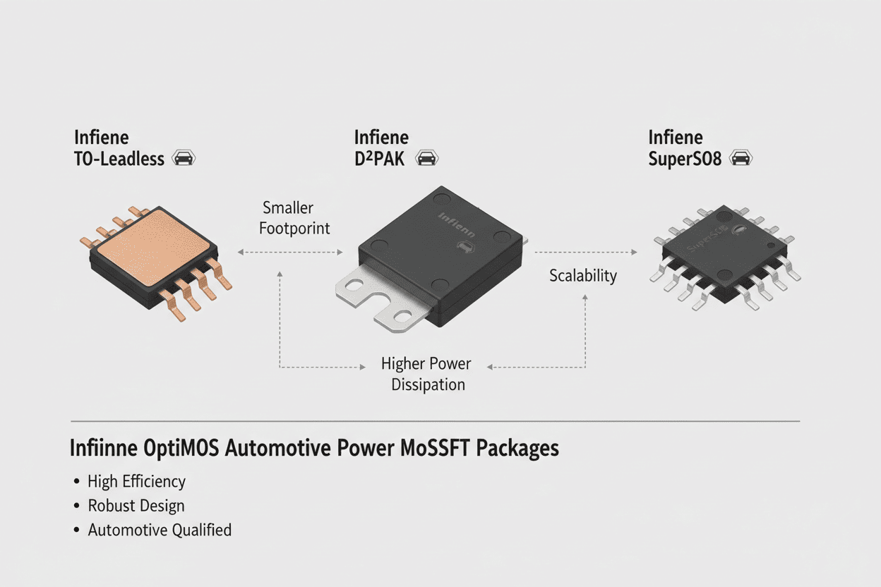
Figure 2: Package technology comparison for automotive MOSFET thermal management
3. Step-by-Step MOSFET Selection Process
3.1 Systematic Selection Methodology
Selecting the optimal MOSFET for automotive power applications requires a systematic approach. Follow this proven process to ensure optimal performance:
Step 1: Define Electrical Requirements
- Determine maximum operating voltage (typically 60V for 48V systems with transients)
- Calculate maximum continuous current and peak current requirements
- Identify switching frequency and duty cycle parameters
- Document any specific safety margin requirements (typically 20-30%)
Step 2: Calculate Power Loss Budget
- Estimate conduction losses: P_cond = I_rms² × RDS(on) × temperature coefficient
- Calculate switching losses: P_sw = 0.5 × V × I × (tr + tf) × f_sw
- Sum total losses and verify against thermal budget
- Target total efficiency >95% for DC-DC converters
Step 3: Select Voltage Rating
- For 48V systems: Choose 60V or 80V devices
- For 12V systems: 40V devices provide optimal cost-performance
- Include margin for load dump transients (up to 58V in 48V systems)
Step 4: Optimize RDS(on) Selection
- Balance RDS(on) vs. cost trade-off
- Consider temperature coefficient (typically 0.4%/°C for OptiMOS)
- Verify current capability at maximum ambient temperature
- Use parallel devices if single device cannot handle current
Step 5: Package and Thermal Design
- Calculate required RthJA based on power dissipation and max TJ
- Select package with adequate thermal performance
- Design PCB with sufficient copper area (recommend 2oz copper)
- Consider thermal vias and heatsinking options
Step 6: Gate Drive Optimization
- Match gate driver capability to MOSFET Qg requirements
- Calculate gate drive power: P_gate = Qg × Vgs × f_sw
- Optimize gate resistance for EMI vs. switching loss trade-off
- Verify dv/dt ratings are not exceeded
3.2 Thermal Design Verification Checklist
Use this checklist to validate your thermal design:
- [ ] Junction temperature calculated at worst-case conditions (T_ambient = 150°C)
- [ ] RDS(on) derating applied using temperature coefficient
- [ ] PCB copper area sufficient for heat spreading
- [ ] Thermal vias placed under device drain pad
- [ ] Thermal interface material selected for module applications
- [ ] Mission profile analysis completed for expected lifetime
- [ ] Safety margin of at least 20°C below maximum TJ maintained
3.3 Design Tools and Resources
Infineon provides comprehensive design support:
- IPOSIM: Online simulation tool for loss and thermal calculations
- MOSFET Power Loss Calculator: Excel-based tool for quick estimations
- Application Notes: Detailed guidance for specific topologies (buck, boost, buck-boost)
- SPICE Models: Accurate simulation models for circuit verification
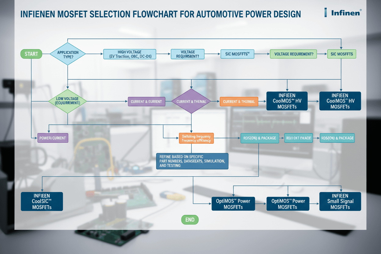
Figure 3: Systematic MOSFET selection flowchart for automotive power applications
4. Real-World Applications and Case Studies
4.1 Application 1: 48V Mild-Hybrid DC-DC Converter
System Requirements:
- Input voltage: 36V-58V (48V nominal)
- Output voltage: 12V
- Output power: 3kW
- Efficiency target: >96%
- Ambient temperature: up to 125°C
Solution Implementation: The design team selected the OptiMOS™ 6 40V (IAUC60N04S6L038) in TO-Leadless package for the high-side and low-side switches. Key specifications:
- RDS(on) = 0.85mΩ at VGS = 10V
- RthJC = 0.45 K/W
- Qg = 78nC
Results Achieved:
- Peak efficiency: 97.2% at 50% load
- Maximum junction temperature: 142°C at full load, 125°C ambient
- Power density: 4.5kW/L
- System passed AEC-Q100 Grade 0 qualification
"The OptiMOS 6 devices enabled us to achieve efficiency targets while maintaining adequate thermal margins in a compact form factor. The TO-Leadless package was critical for achieving the required power density." — Lead Power Electronics Engineer, Tier 1 Automotive Supplier
4.2 Application 2: 12V Start-Stop System
System Requirements:
- Battery voltage: 6V-16V (12V nominal)
- Cranking current: 150A peak
- Continuous current: 80A
- Ambient temperature: up to 150°C under-hood
- Package: Must fit existing relay footprint
Solution Implementation: Two OptiMOS™ 5 40V (IAUC120N04S5N019) devices in parallel in SuperSO8 package replaced the mechanical relay:
- RDS(on) = 1.15mΩ per device (0.575mΩ effective)
- Combined RthJA = 15 K/W on optimized PCB
- Total gate charge: 2 × 45nC = 90nC
Results Achieved:
- Voltage drop at 150A: 86mV (vs. 200mV for mechanical relay)
- Power savings: 17W during cranking events
- Elimination of relay contact wear and arcing
- System lifetime extended from 300k to >2M cycles
4.3 Application 3: Electric Power Steering (EPS) Motor Drive
System Requirements:
- DC link voltage: 12V
- Phase current: 100A RMS, 200A peak
- Switching frequency: 20kHz
- Safety: ASIL-D compliance required
- Efficiency: >98% at rated power
Solution Implementation: Six OptiMOS™ 6 40V (IAUC80N04S6L044) devices configured in a three-phase bridge:
- RDS(on) = 0.95mΩ
- Excellent body diode reverse recovery characteristics
- AEC-Q101 Grade 0 qualified
Results Achieved:
- System efficiency: 98.5% at rated operating point
- Smooth motor control with minimal torque ripple
- Thermal performance allowed elimination of active cooling
- ASIL-D safety requirements met through redundant monitoring
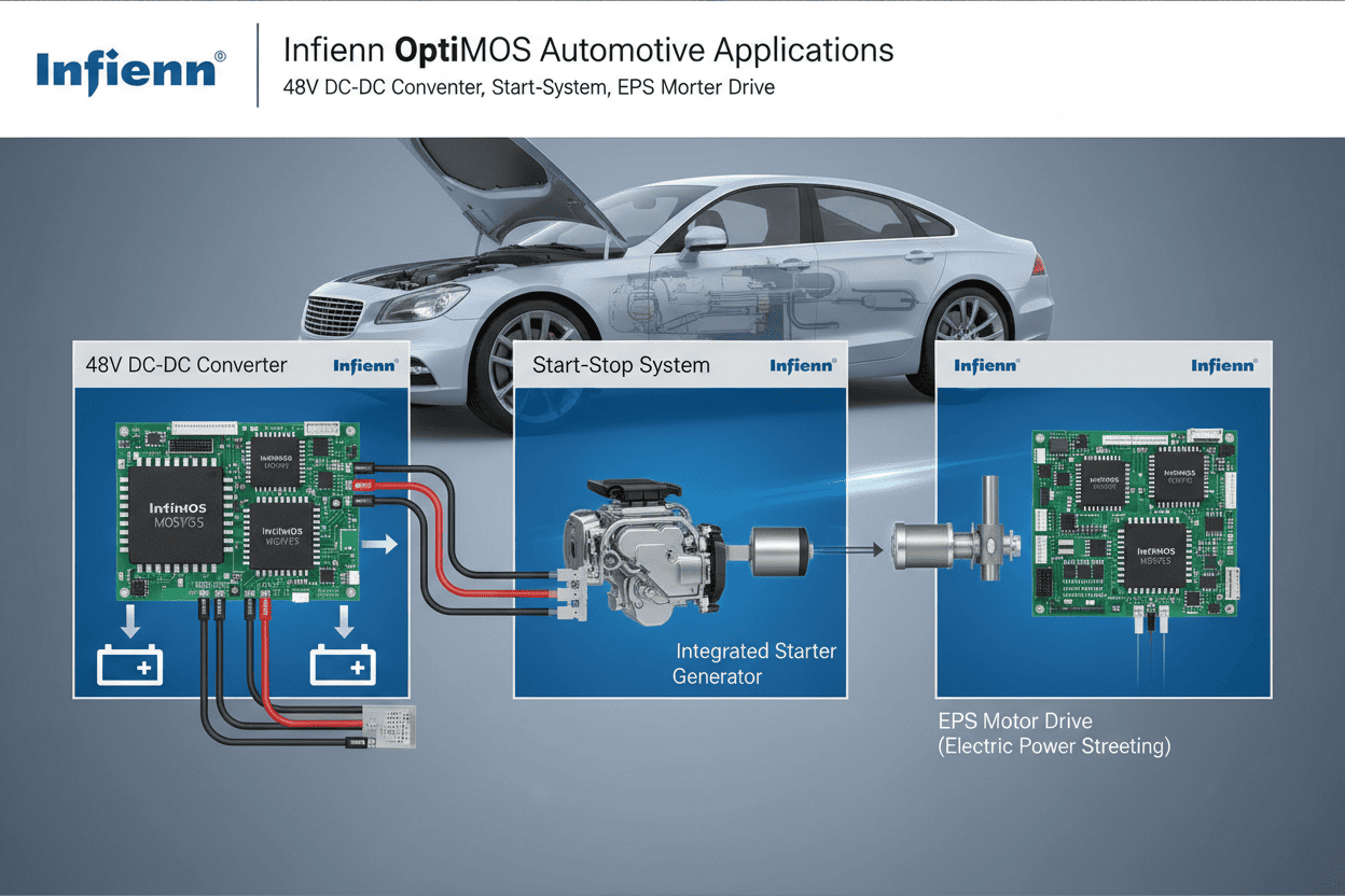
Figure 4: Real-world automotive applications of Infineon OptiMOS devices
5. Frequently Asked Questions
What is the difference between automotive-grade and industrial-grade MOSFETs?
Automotive-grade MOSFETs (AEC-Q101 qualified) undergo significantly more rigorous testing compared to industrial-grade devices. Key differences include:
- Temperature range: Automotive devices are qualified for -55°C to +175°C operation
- Quality requirements: Automotive devices require zero defect strategies and PPAP documentation
- Traceability: Full lot traceability required for automotive applications
- Testing: Additional HTRB, temperature cycling, and HAST testing for automotive qualification
Infineon OptiMOS automotive devices meet all AEC-Q101 requirements and are supported with complete PPAP documentation packages.
How do I calculate the maximum allowable RDS(on) for my application?
To determine the maximum RDS(on) for your specific application:
- Identify your maximum allowable power dissipation: P_max = (T_junction_max - T_ambient) / RthJA
- Calculate maximum RDS(on) at elevated temperature: RDS(on)_max = P_max / I_rms²
- Apply temperature coefficient correction: RDS(on)_25C = RDS(on)_max / (1 + TC × (T_junction - 25))
For example, with T_ambient = 125°C, T_junction_max = 175°C, RthJA = 20 K/W, and I_rms = 50A:
- P_max = (175 - 125) / 20 = 2.5W
- RDS(on)_max = 2.5 / 2500 = 1.0mΩ at 175°C
- RDS(on)_25C = 1.0 / 1.6 = 0.625mΩ (using 0.4%/°C coefficient)
Can I parallel MOSFETs to increase current capability?
Yes, paralleling MOSFETs is a common practice in automotive power applications. However, several factors must be considered:
- Current sharing: Use individual gate resistors (1-5Ω) to prevent oscillations
- Layout symmetry: Ensure equal trace lengths and impedances to each device
- Thermal coupling: Devices should be thermally coupled to prevent thermal runaway
- Gate drive capability: Verify gate driver can supply sufficient current for parallel Qg
Infineon's TO-Leadless package is particularly well-suited for paralleling due to its low package inductance and excellent thermal performance.
What thermal management techniques work best for automotive MOSFETs?
Effective thermal management strategies include:
- PCB design: Use 2oz or 3oz copper with large copper areas for heat spreading
- Thermal vias: Place multiple vias under the drain pad to transfer heat to inner layers
- Heatsinking: For high-power applications, consider aluminum-core PCBs or external heatsinks
- Thermal interface materials: Use high-performance TIMs for module applications
- Airflow: Where possible, leverage vehicle airflow for additional cooling
Infineon's application note AN_2023_034 provides detailed thermal design guidelines for automotive MOSFET implementations.
How does RDS(on) change over the device lifetime?
RDS(on) can increase over the device lifetime due to various degradation mechanisms:
- Hot carrier injection: Can cause 5-15% RDS(on) increase over 10 years
- Temperature cycling: Solder joint degradation affects thermal resistance
- Electrical stress: Gate oxide degradation can affect threshold voltage
Infineon OptiMOS devices are designed with robust process technologies that minimize these effects. End-of-life RDS(on) is typically guaranteed to be within 120% of initial specifications under normal operating conditions.
6. Conclusion: Powering the Future of Automotive Electronics
Key Takeaways
This comprehensive analysis of Infineon OptiMOS automotive MOSFET selection reveals several critical insights for engineers designing 48V/12V automotive power systems:
- RDS(on) optimization directly impacts system efficiency, with every milliohm reduction translating to significant power savings and improved thermal performance
- Package selection is equally important as die selection—TO-Leadless packages offer superior thermal performance in compact footprints
- Thermal design must account for worst-case automotive environments, with ambient temperatures reaching 150°C
- AEC-Q101 qualification ensures devices can withstand the harsh automotive environment for the vehicle's entire lifetime
The transition to 48V mild-hybrid systems and advanced 12V architectures demands power semiconductors that deliver exceptional performance under extreme conditions. Infineon's OptiMOS portfolio, with industry-leading RDS(on) specifications and comprehensive automotive qualification, provides engineers with the tools needed to meet these challenges.
Next Steps for Your Design
Ready to optimize your automotive power system design? Here's how to proceed:
- Use Infineon's IPOSIM tool to simulate losses and thermal performance for your specific application
- Request samples of recommended OptiMOS devices through Infineon's distribution partners
- Download application notes AN_2023_034 and AN_2022_018 for detailed design guidance
- Contact Infineon's technical support team for personalized assistance with your specific requirements
"The future of automotive electrification depends on continuous innovation in power semiconductor technology. Infineon remains committed to delivering OptiMOS solutions that enable our customers to achieve higher efficiency, greater power density, and uncompromising reliability in their automotive power systems." — Infineon Technologies AG
Ready to optimize your automotive power design? Visit Infineon's Automotive MOSFET product page to explore the complete OptiMOS portfolio, access simulation tools, and request technical support for your next project.