


Switch Mode Power Supply (SMPS): Complete Selection and Design Guide for Engineers
Switch mode power supplies have become the backbone of modern electronic systems, from consumer devices to industrial automation. For design engineers and procurement teams evaluating power solutions, understanding SMPS technology—and knowing how to select the right topology for your application—directly impacts efficiency, reliability, and cost.
This guide explains the key technical parameters that matter, walks through selection methodology based on real design constraints, and highlights common pitfalls that can derail your power stage performance. Whether you're designing automotive electronics, IoT sensor nodes, or industrial control systems, you'll find actionable insights to make better power supply decisions.
Table of Contents
- What is a Switch Mode Power Supply and Why It Matters
- Key Technical Parameters Explained
- How to Choose the Right SMPS Topology for Your Application
- Performance Comparison: Buck, Boost, Buck-Boost, and Isolated Topologies
- Design Considerations and Common Pitfalls
- Supply Chain and Sourcing Considerations
- FAQ
- Conclusion and Recommended Next Steps
1. What is a Switch Mode Power Supply and Why It Matters
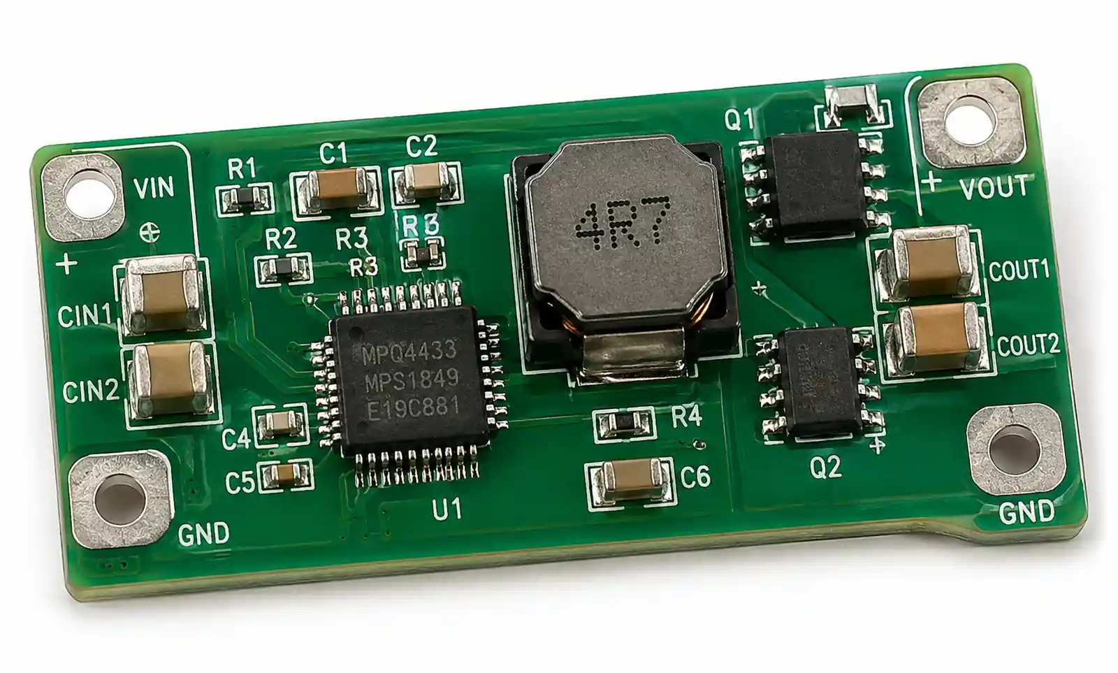
A switch mode power supply converts electrical power efficiently by switching a power transistor on and off at high frequency, typically between 20 kHz and several MHz. Unlike linear regulators that dissipate excess voltage as heat, SMPS topologies transfer energy through inductors and capacitors, achieving efficiencies above 85% and often exceeding 95% in optimized designs.
For engineers, this efficiency translates to reduced thermal management requirements, smaller form factors, and lower operating costs. In battery-powered applications, SMPS efficiency directly extends runtime. In industrial systems drawing continuous power, efficiency improvements reduce heat dissipation and improve long-term reliability.
The trade-off is complexity. SMPS designs require careful component selection, PCB layout discipline, and attention to electromagnetic interference (EMI). Design mistakes—such as inadequate loop compensation or poor inductor placement—can cause instability, excessive ripple, or conducted/radiated emissions that fail regulatory testing.
2. Key Technical Parameters Explained
When evaluating SMPS controllers or integrated modules, focus on parameters that directly affect your design's performance, reliability, and compliance. The datasheet contains dozens of specs, but these are the ones that typically drive selection decisions.
Efficiency and Power Loss
Efficiency is the ratio of output power to input power, expressed as a percentage. Modern synchronous buck converters achieve 92-96% efficiency at mid-load, while flyback converters in isolated applications typically reach 80-88%. Switching losses, conduction losses, and gate drive losses all contribute to total power dissipation.
Pay attention to efficiency curves across the full load range. Many SMPS controllers maintain high efficiency at heavy loads but drop significantly at light loads unless they implement pulse-skipping or burst mode operation. For battery applications with variable load profiles, light-load efficiency matters as much as peak efficiency.
Switching Frequency
Switching frequency affects inductor size, capacitor selection, and EMI characteristics. Higher frequencies (above 1 MHz) enable smaller passive components, reducing solution size. However, switching losses increase with frequency, and EMI mitigation becomes more challenging.
In automotive and industrial applications requiring conducted emissions compliance (CISPR 25, CISPR 32), frequency selection is a critical design trade-off. Operating below AM radio bands (530-1710 kHz) or above 2 MHz can simplify filtering, but component availability and cost constraints often push designs into the 300-600 kHz range.
Input and Output Voltage Range
SMPS controllers specify minimum and maximum input voltages, and some topologies impose strict limits on input-to-output voltage ratios. Buck converters require Vin > Vout, boost converters require Vout > Vin, and buck-boost or SEPIC topologies handle overlapping input-output ranges at the cost of additional components and slightly lower efficiency.
In automotive applications, the input voltage range must accommodate cold-crank (as low as 3.5V), normal operation (9-16V), and load dump transients (up to 40V). Industrial systems on 24V rails must tolerate ±20% variation. Always verify that the controller's operating range covers your worst-case transients, not just nominal voltage.
Load Regulation and Line Regulation
Load regulation specifies how much the output voltage changes as load current varies from minimum to maximum. Line regulation specifies output voltage variation as input voltage changes. High-performance applications require tight regulation, typically under 1% for both metrics.
These parameters are influenced by the feedback loop design, reference accuracy, and output impedance. If your application has strict voltage tolerance requirements—such as powering precision ADCs or RF front-ends—verify that the SMPS controller's regulation performance meets your needs without requiring additional post-regulation.
Transient Response
Transient response describes how quickly the SMPS recovers from sudden load changes. Critical in applications with pulsed loads—such as wireless transceivers that switch between sleep and transmit modes, or processors that clock-gate execution blocks. Poor transient response causes voltage droop or overshoot that can trigger brownout resets or damage sensitive circuitry.
Compensation network design directly affects transient response. Controllers with adaptive on-time or voltage-mode control may require different compensation strategies than current-mode controllers. When selecting an SMPS, review the datasheet's recommended compensation components and verify transient performance under your expected load step conditions.
| Parameter | Typical Range | Impact on Design |
|---|---|---|
| Efficiency (full load) | 85-96% | Thermal management, battery life |
| Switching frequency | 200 kHz - 2 MHz | Component size, EMI filtering complexity |
| Input voltage range | Application-specific | Topology selection, transient protection |
| Output voltage accuracy | ±1% to ±5% | Post-regulation requirements, sensitive loads |
| Load transient response | 10-100 µs | Bulk capacitance, compensation network |
| Quiescent current | 10 µA - 5 mA | Battery standby life, light-load efficiency |
| Operating temperature | -40°C to +125°C | Automotive/industrial qualification |
This table summarizes the parameters most frequently used in SMPS selection decisions. Prioritize parameters based on your application constraints—battery life for portable devices, thermal performance for high-density systems, transient response for RF applications.
3. How to Choose the Right SMPS Topology for Your Application
Selecting an SMPS topology begins with your input voltage range, required output voltage, load current, and isolation requirements. No single topology optimizes every application, so the selection process involves trade-offs between efficiency, cost, component count, and design complexity.
Step 1: Define Input-Output Voltage Relationship
If your output voltage is always lower than the minimum input voltage, a buck (step-down) converter is the natural choice. If output must be higher than input, use a boost (step-up) converter. When input and output voltages overlap, or when input can be higher or lower than output, consider buck-boost, SEPIC, or Cuk topologies.
For applications requiring galvanic isolation—such as AC-DC converters, medical devices, or systems with ground loop concerns—isolated topologies like flyback, forward, or LLC resonant converters are necessary. Isolation adds complexity and cost, so only specify it when safety standards or system architecture require it.
Step 2: Evaluate Efficiency Requirements
If your application demands peak efficiency above 90%, synchronous rectification is typically required. Synchronous buck converters replace the freewheeling diode with a low-RDS(on) MOSFET, reducing conduction losses. This is standard in battery-powered devices, data center power supplies, and any application where thermal constraints limit power dissipation.
For cost-sensitive designs where efficiency in the 80-85% range is acceptable, asynchronous (diode-based) topologies reduce component count and simplify PCB layout. This is common in auxiliary power supplies, bias rails, and low-power industrial systems.
Step 3: Consider Component Size and PCB Area
Switching frequency directly impacts passive component size. Operating at 1-2 MHz enables 1-2 µH inductors in compact packages, while 200-400 kHz designs require 4-10 µH inductors. Higher frequency reduces magnetics size but increases switching losses and EMI filtering requirements.
In space-constrained designs—wearables, IoT sensors, portable medical devices—integrated power modules that combine controller, MOSFETs, and inductor in a single package offer the smallest footprint. The trade-off is reduced flexibility in optimizing efficiency or transient response.
Step 4: Assess EMI and Noise Sensitivity
Switch mode converters generate high-frequency noise that can couple into sensitive analog circuits, RF front-ends, or precision measurement systems. If your design includes ADCs with resolution above 12 bits, low-noise amplifiers, or RF transceivers, conducted and radiated noise from the SMPS can degrade signal integrity.
Mitigation strategies include spread-spectrum clocking (frequency dithering to reduce peak emissions), synchronous operation (clocking multiple converters from a common source to avoid beat frequencies), and careful PCB layout with ground planes and proper decoupling. Some applications require post-regulation with low-dropout linear regulators to isolate sensitive analog stages from SMPS ripple.
| Application Type | Recommended Topology | Key Design Priority |
|---|---|---|
| Battery-powered IoT device (3.7V input, 3.3V output) | Synchronous buck | Light-load efficiency, quiescent current |
| Automotive 12V rail to 5V USB (cold-crank to load dump) | Synchronous buck with wide Vin | Transient protection, efficiency |
| Battery charger (5V input, 4.2V Li-ion) | Buck or linear (if thermal acceptable) | Charge accuracy, cost |
| Isolated AC-DC adapter (85-265 VAC to 12V DC) | Flyback | Safety isolation, cost |
| Boost for LED backlight (3.3V to 24V) | Synchronous boost | High output voltage, efficiency |
| Industrial 24V to 12V/5V dual output | Synchronous buck + LDO or buck + buck | Efficiency, load regulation |
| Medical device (isolated, low leakage) | Isolated flyback or forward | Safety compliance, leakage current |
This selection matrix shows typical topology choices for common applications. Use it as a starting point, then refine based on specific performance requirements, cost targets, and regulatory constraints.
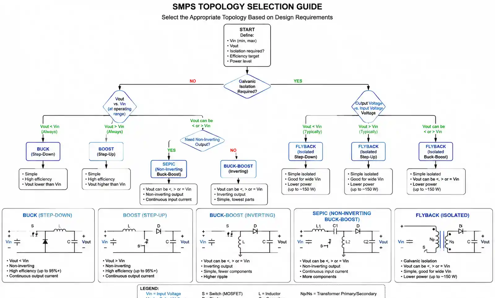
4. Performance Comparison: Buck, Boost, Buck-Boost, and Isolated Topologies
Each SMPS topology has characteristic strengths and limitations. Understanding these trade-offs helps you match topology to application requirements and avoid overengineering.
Buck (Step-Down) Converter
Buck converters step down input voltage to a lower output voltage with typical efficiencies of 90-95% in synchronous designs. Pros include simple control, predictable behavior, and straightforward compensation. Cons include the requirement that Vin > Vout at all times, and sensitivity to input voltage transients.
Best for: Battery-powered devices, point-of-load regulation, powering digital logic from higher-voltage rails.
Boost (Step-Up) Converter
Boost converters step up voltage with similar efficiency to buck converters, but output current is lower than input current. Boost converters have a right-half-plane zero in their transfer function, complicating loop compensation and limiting transient response. Boost topology cannot limit inrush current at startup without additional components.
Best for: LED drivers, battery backup systems, generating bias voltages higher than input supply.
Buck-Boost and SEPIC Converters
Buck-boost, SEPIC, and Cuk topologies can step voltage up or down, making them ideal when input voltage range crosses output voltage. The trade-off is increased component count (two inductors in SEPIC/Cuk, or higher inductor current stress in buck-boost), slightly lower efficiency, and more complex magnetics design.
Best for: Automotive applications with wide input variation, single-cell Li-ion to 5V conversion, systems where input source voltage is uncertain.
Flyback Converter (Isolated)
Flyback is the most common isolated topology for low-to-medium power levels (under 100W). It provides galvanic isolation with a single magnetic component (coupled inductor/transformer), but efficiency is typically 80-88%, and output ripple is higher than non-isolated converters. Flyback converters require careful transformer design and snubber circuits to manage leakage inductance.
Best for: AC-DC adapters, isolated bias supplies, medical devices requiring safety isolation.
| Topology | Efficiency (typical) | Component Count | Complexity | Isolation | Best Use Cases |
|---|---|---|---|---|---|
| Synchronous Buck | 92-96% | Low | Low | No | Battery-powered, point-of-load |
| Asynchronous Buck | 85-90% | Very Low | Very Low | No | Cost-sensitive, auxiliary rails |
| Synchronous Boost | 90-95% | Low | Medium | No | LED drivers, battery backup |
| Buck-Boost | 85-92% | Medium | Medium | No | Wide input voltage range |
| SEPIC | 85-90% | Medium | Medium | No | Vin crosses Vout |
| Flyback (isolated) | 80-88% | Medium | High | Yes | AC-DC, isolated bias, medical |
| Forward (isolated) | 85-90% | High | High | Yes | Higher power, multiple outputs |
This comparison table highlights the primary trade-offs between common SMPS topologies. Choose based on your specific efficiency targets, cost constraints, and isolation requirements rather than assuming one topology is universally superior.
5. Design Considerations and Common Pitfalls
Even with the right topology and controller IC, SMPS designs fail or underperform due to preventable mistakes in component selection, PCB layout, and loop compensation. These are the issues encountered most frequently in design validation and failure analysis.
Inductor Selection Mistakes
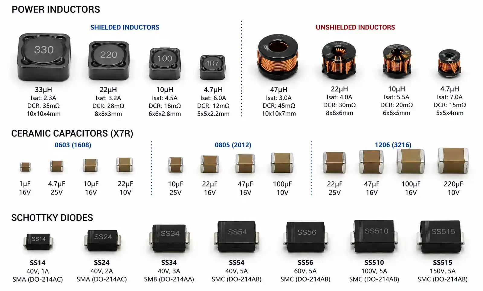
Choosing an inductor based only on inductance value and current rating is insufficient. Saturation current (Isat) must exceed peak inductor current with margin, and DC resistance (DCR) directly impacts efficiency. In high-current designs, a 10 mΩ difference in DCR can cost 1-2% efficiency.
Core material matters for high-frequency operation. Ferrite cores work well above 500 kHz, while powdered iron cores are better for lower frequencies but have higher core losses. Shielded inductors reduce radiated EMI but cost more and may have lower saturation current than unshielded types. Always verify inductor performance at your operating frequency and temperature.
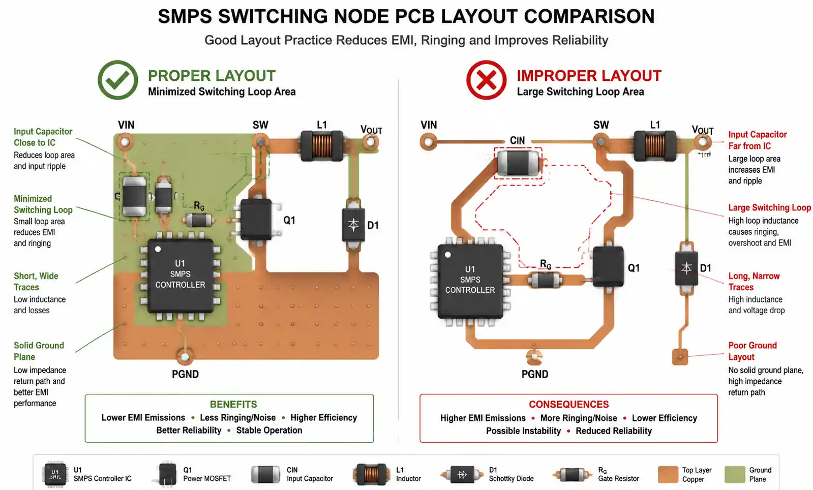
PCB Layout Errors
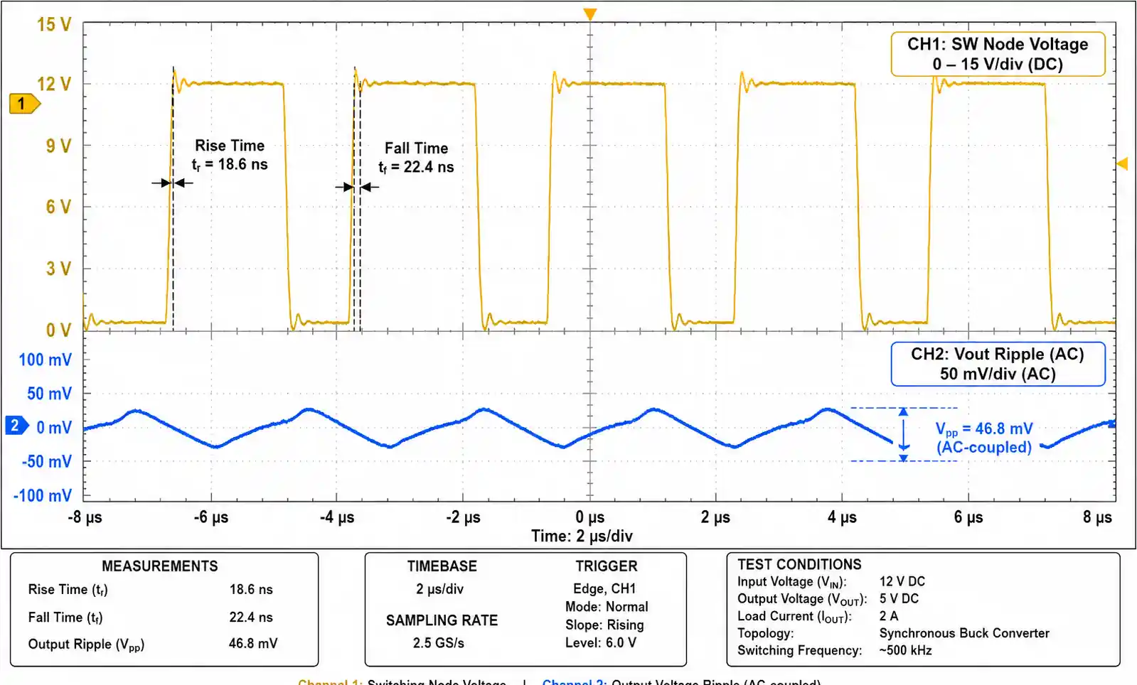
SMPS PCB layout mistakes are the leading cause of noise, instability, and EMI failures. The switching node—the connection between the switch transistor, inductor, and freewheeling diode or synchronous FET—carries high di/dt current and must be minimized in area. A large switching node loop acts as an antenna, radiating noise and coupling into sensitive circuits.
Place input and output capacitors as close as possible to the IC power pins. Use ground planes, but do not run high-frequency switching currents through narrow traces or split ground planes. Dedicate a solid ground plane area for power stage components, and connect analog feedback and control circuitry to a quiet ground point (typically the output capacitor negative terminal).
Insufficient Input/Output Capacitance
Input capacitors must handle the RMS ripple current of the converter, which can be substantial in buck converters. Ceramic capacitors (X5R or X7R) with low ESR are preferred, but multiple capacitors in parallel may be required to meet ripple current rating. Underestimating ripple current causes premature capacitor failure and increased input voltage ripple.
Output capacitance sets output voltage ripple and transient response. In applications with fast load transients, bulk capacitance must be sufficient to supply load current during the feedback loop's response time. Tantalum or polymer electrolytic capacitors provide higher capacitance density than ceramics, but watch ESR and ESL at high frequencies.
Loop Compensation Errors
SMPS controllers typically operate in voltage-mode or current-mode control, each requiring different compensation strategies. Insufficient phase margin (less than 45 degrees) causes ringing and potential instability. Excessive phase margin (over 70 degrees) yields sluggish transient response.
Many engineers rely on datasheet reference designs without validating loop stability under their specific operating conditions. Input voltage, output voltage, load current, and even PCB parasitics affect loop dynamics. For production designs, measure loop response with a network analyzer or perform load transient testing to verify stability margins.
| Common Pitfall | Consequence | Mitigation |
|---|---|---|
| Inductor saturation at peak current | Efficiency loss, overheating, potential damage | Select Isat > 1.3× peak inductor current |
| Large switching node loop area | Radiated EMI, crosstalk | Minimize loop area, use ground plane |
| Inadequate input capacitor ripple current rating | Capacitor overheating, failure | Sum RMS ripple current, parallel multiple caps |
| Poor feedback trace routing | Noise injection, instability | Route feedback traces away from switching node |
| Ignoring thermal design | Controller or MOSFET overheating | Calculate power dissipation, use thermal vias |
| Skipping load transient testing | Instability under real load conditions | Test with dynamic load, verify voltage deviation |
This table lists the most frequently encountered design mistakes and their consequences. Address these systematically during design review to avoid costly board respins or field failures.
6. Supply Chain and Sourcing Considerations
Power management ICs and passive components for SMPS designs face supply chain challenges that can impact project timelines and costs. Proactive sourcing strategies and design-for-availability practices reduce risk.
Controller IC Availability and Lead Times
High-volume power management ICs from major suppliers (Texas Instruments, Analog Devices, Infineon, ON Semiconductor) typically have better availability than niche or single-source parts. During component shortages, lead times for specialized SMPS controllers can extend to 26-52 weeks.
Design with second-source options when possible. Many buck and boost controllers have pin-compatible or functionally equivalent alternatives. If your design relies on a single-source part, maintain higher inventory buffers or identify drop-in replacements early in the design cycle.
Passive Component Sourcing
Inductors are often the most supply-constrained SMPS components, particularly in automotive-grade or high-current ratings. Custom magnetics have longer lead times than catalog parts. Standardize on inductors from multiple suppliers (Coilcraft, Wurth, TDK, Murata) to maintain sourcing flexibility.
Ceramic capacitors with specific voltage ratings and capacitance values in compact case sizes (0603, 0805) can face allocation during market tightness. Design with standard capacitance values and avoid pushing voltage derating limits too close—use 25V rated capacitors for 12V applications rather than 16V parts.
Cost Optimization Without Compromising Performance
In high-volume production, even small component cost reductions multiply. However, optimizing cost by selecting cheaper inductors with higher DCR or lower-grade capacitors with higher ESR can degrade efficiency and long-term reliability.
Balance cost and performance by targeting efficiency at typical load rather than peak load, accepting slightly larger component size to use more readily available parts, or simplifying control features (e.g., fixed-frequency operation instead of spread-spectrum) if EMI requirements allow.
| Component Type | Availability Risk | Mitigation Strategy |
|---|---|---|
| SMPS controller IC | Medium | Design with pin-compatible alternates |
| Power MOSFETs | Low-Medium | Multiple approved sources, standard packages |
| Inductors (specialty) | High | Catalog parts from multiple vendors, early procurement |
| High-capacitance ceramics | Medium | Standard values, multiple case sizes approved |
| Schottky/sync rectifiers | Low | Commodity parts, multiple sources |
This table summarizes supply chain risks for typical SMPS components. For critical designs, engage with distributors early to understand lead times and allocations, and consider consignment inventory for long-lead components.
7. FAQ
What is the difference between synchronous and asynchronous SMPS?
Synchronous SMPS replaces the freewheeling diode with a MOSFET, reducing conduction losses and improving efficiency by 3-8%. Asynchronous designs use a Schottky diode, which is simpler and lower cost but dissipates more power. Choose synchronous for battery-powered or thermally constrained applications, asynchronous for cost-sensitive auxiliary supplies.
How do I calculate the required inductor value for a buck converter?
Inductor value depends on switching frequency, input/output voltage, load current, and desired ripple current. A common design target is 20-40% ripple current. Use the formula: L = (Vout × (Vin - Vout)) / (Vin × ΔIL × Fsw), where ΔIL is ripple current and Fsw is switching frequency. Verify saturation current rating exceeds peak current.
Can SMPS be used in automotive applications?
Yes, but automotive SMPS designs must meet AEC-Q100 qualification for ICs, handle cold-crank voltage drops to 3.5V, survive load dump transients up to 40V, and comply with conducted/radiated emissions standards (CISPR 25). Use automotive-grade components and include input transient protection.
What causes SMPS instability or oscillation?
Instability typically results from insufficient loop compensation, excessive phase lag in the feedback network, or PCB layout issues that introduce noise into the feedback path. Verify phase margin exceeds 45 degrees across the operating range. Poor grounding or large parasitic inductance in the output capacitor can also cause oscillation.
How do I reduce EMI from a switch mode power supply?
Use spread-spectrum clocking if the controller supports it, minimize switching node loop area on the PCB, add input and output filters (common-mode chokes, X/Y capacitors), use shielded inductors, and implement proper grounding with continuous planes. Slower switching edges reduce EMI but increase switching losses—balance based on your emissions limits.
What is the impact of operating temperature on SMPS performance?
Efficiency decreases at high temperatures due to increased MOSFET RDS(on) and inductor DCR. Controller quiescent current may increase, affecting light-load efficiency. Capacitor ESR increases, degrading ripple performance. Always verify thermal design ensures junction temperatures remain within datasheet limits under worst-case ambient and load conditions.
Are there pin-compatible alternatives if my SMPS controller goes obsolete?
Many buck and boost controllers have functional equivalents from competing suppliers, though exact pin compatibility is rare. When designing, document critical parameters (switching frequency, feedback topology, compensation network) so equivalent parts can be evaluated. Some manufacturers offer longevity programs guaranteeing availability for 10+ years in industrial/automotive applications.
What testing is required to validate SMPS design?
At minimum, test efficiency across load range, line and load regulation, transient response to load steps, input/output ripple, and thermal performance under maximum load. For compliance-critical applications, conduct conducted and radiated emissions testing (EMI), load dump and cold-crank testing (automotive), and safety isolation testing (medical/AC-DC).
8. Conclusion and Recommended Next Steps
Selecting and designing with switch mode power supplies requires balancing efficiency, cost, component availability, and design complexity against your application's specific requirements. Buck converters dominate point-of-load regulation in battery-powered and digital systems due to high efficiency and design simplicity. Boost converters serve LED drivers and battery backup applications. Buck-boost and isolated topologies address wide input ranges and safety isolation requirements at the cost of additional components and design effort.
If your application prioritizes efficiency and operates from a stable input voltage higher than your output requirement, start with a synchronous buck converter. If input voltage varies widely or crosses your target output voltage, evaluate buck-boost or SEPIC topologies. For isolated designs, flyback converters offer the best balance of cost and performance below 100W.
Before finalizing your design, validate loop stability under worst-case operating conditions, verify thermal performance with realistic load profiles, and conduct EMI pre-compliance testing if your product faces regulatory requirements. Engage with component suppliers early to understand lead times for inductors and specialty ICs, and design with second-source options to reduce supply chain risk.
For further technical support, consult application notes from major SMPS controller manufacturers, download reference designs that match your topology and power level, and consider using online design tools that automate component selection and loop compensation calculations. If your design involves high power levels (above 100W), isolated topologies, or stringent EMI requirements, consulting with a field applications engineer (FAE) can prevent costly design iterations.