


Tunnel Diode Explained in Practice Working Principle Behavior and Real Applications
The tunnel diode, also known as the Esaki diode, is a semiconductor device built on quantum tunneling rather than traditional carrier diffusion. Because of its extremely thin junction and heavy doping, it exhibits negative differential resistance and very fast response. This article looks at the device from an engineering perspective, focusing on how it actually behaves in circuits, where it works best, and what limitations need to be considered during design.
Table of Contents
- Introduction to Tunnel Diodes
- Historical Background
- Symbol and Representation
- Device Structure and Physics
- Operating Principle
- V–I Characteristics and Negative Resistance
- Equivalent Circuit Model
- Advantages and Limitations
- Applications in Modern Circuits
- Tunnel Diode vs PN Junction Diode
- Selection Guidelines
- FAQ
Introduction to Tunnel Diodes
A tunnel diode is a heavily doped PN junction device where carriers move through the junction using quantum tunneling. Unlike a standard diode, it does not rely purely on overcoming a potential barrier.
In practical terms:
- The depletion region is extremely thin
- Electrons can pass through without needing high energy
- The device reacts very quickly to voltage changes
Because of this, tunnel diodes are often considered when speed matters more than power.
Historical Background
The device was discovered in 1957 by Leo Esaki during experiments on heavily doped semiconductors. At the time, the observed current behavior did not match classical theory, which led to the explanation using quantum tunneling.
Tunnel diodes saw early use in microwave circuits, especially before high-speed transistors became widely available. Today, they are less common but still useful in specific high-frequency designs.
Symbol and Representation
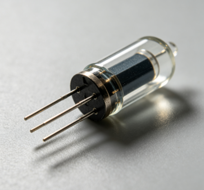
The schematic symbol is close to a standard diode, but includes slight modifications to indicate its non-linear and negative resistance behavior. It still uses anode and cathode terminals like any diode.
Device Structure and Physics
Structural details
- Very high doping concentration on both sides
- Extremely narrow depletion layer
- High carrier density
What this means in practice
The heavy doping causes the energy bands to overlap slightly. Because of this, electrons do not need to climb over a barrier—they can tunnel through it directly. This is the key reason the device behaves differently from a normal diode.
Operating Principle
Instead of thinking only in terms of current flow, it helps to look at how the device responds as voltage changes.
No bias
Carrier movement exists in both directions, so net current is essentially zero.
Small forward voltage
Tunneling begins and current increases quickly.
Peak point
The current reaches its maximum value.
Negative resistance region
As voltage increases further, tunneling becomes less efficient. Current drops even though voltage rises.
Higher forward voltage
Normal diode conduction takes over and current increases again.
Reverse bias
Unlike a standard diode, current still flows easily due to tunneling.
V–I Characteristics and Negative Resistance
The V–I curve is what makes this device stand out.
Key observations:
- A clear peak current point
- A region where current decreases with increasing voltage
- A return to normal behavior at higher voltages
This negative resistance region is not just a curiosity—it is what enables oscillator and RF applications.
Equivalent Circuit Model
In circuit design, the tunnel diode is often modeled using:
- A negative resistance element
- Junction capacitance
- Small series resistance
- Parasitic inductance
These elements become especially important in high-frequency designs, where even small parasitics can shift performance.
Advantages and Limitations
Advantages
- Very fast response time
- Works well at high frequency
- Low voltage operation
- Compact structure
Limitations
- Cannot handle large power
- Narrow usable region
- Sensitive to temperature
- Requires careful bias control
In real designs, these limitations often define whether the device is practical.
Applications in Modern Circuits
Tunnel diodes are not widely used in general electronics anymore, but they still appear in areas where their unique behavior is useful:
- Microwave oscillators
- RF signal amplification
- High-speed switching
- Frequency conversion circuits
- Radar and communication systems
They are particularly useful when a simple, fast, and stable oscillation source is needed.
Tunnel Diode vs PN Junction Diode
| Feature | Tunnel Diode | PN Junction Diode |
|---|---|---|
| Doping Level | Extremely high | Moderate |
| Depletion Region | Very thin | Wider |
| Operating Mechanism | Quantum tunneling | Carrier diffusion |
| Speed | Very fast | Slower |
| Negative Resistance | Yes | No |
| Power Handling | Low | Higher |
| Reverse Current | High | Low |
Selection Guidelines
When choosing a tunnel diode, engineers typically check:
- Frequency range capability
- Peak and valley current values
- Voltage levels for operation
- Junction capacitance
- Thermal behavior
- Package size and parasitics
A mismatch in these parameters can easily lead to unstable circuit behavior.
FAQ
1. Why does current drop in the negative resistance region
Because fewer electrons are able to tunnel as the energy bands move out of alignment.
2. Is the tunnel diode still relevant today
Yes, mainly in RF and microwave designs where speed is critical.
3. Why is heavy doping necessary
It reduces the barrier width enough for tunneling to occur.
4. Can it replace a standard diode
No, it serves a very different purpose and is not suitable for general rectification.
5. What is the biggest limitation
Low power handling and a narrow operating range make it less flexible than modern devices.
Conclusion
The tunnel diode is not a general-purpose component, but it remains an important device in specific areas of electronics. Its behavior is tied directly to quantum effects, which gives it capabilities that conventional devices do not have. For engineers working with high-frequency or fast-switching circuits, understanding how it works can still be valuable.